Semiconductor memory device, method of writing data therein, and method of reading data therefrom

Active Publication Date: 2008-12-11
RENESAS ELECTRONICS CORP
View PDF6 Cites 0 Cited by
  • Summary
  • Abstract
  • Description
  • Claims
  • Application Information

AI Technical Summary

Benefits of technology

[0010]In the semiconductor memory device, the number of the conductive plugs electrically connected to the source region of the second field-effect transistor and the number of the conductive plugs electrically connected to the drain region are different. Therefore, by passing current through the conductive plugs the number of which is smaller, the resistance of the conductive plugs can be easily increased. This change in resistance appears as change in output (potential or current) of the second field-effect transistor. Therefore, by detecting by the detection circuit the difference between the output of the first field-effect transistor and the output of the second field-effe

Problems solved by technology

Therefore, the semiconductor memory device described above

Method used


Image

  • Semiconductor memory device, method of writing data therein, and method of reading data therefrom
  • Semiconductor memory device, method of writing data therein, and method of reading data therefrom
  • Semiconductor memory device, method of writing data therein, and method of reading data therefrom

Examples


Example

First Embodiment

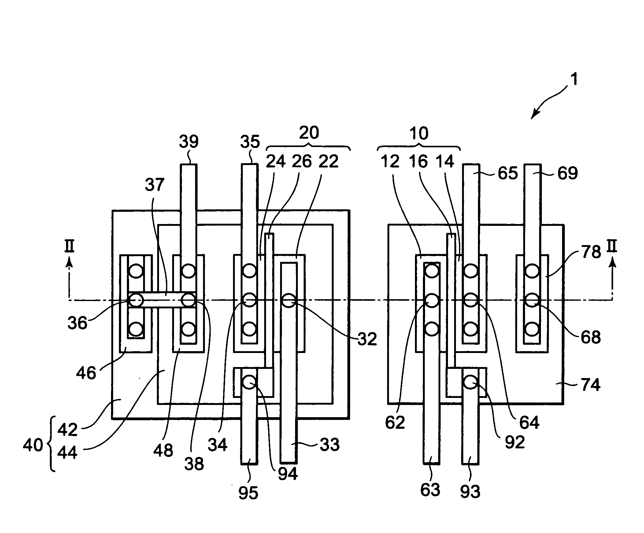
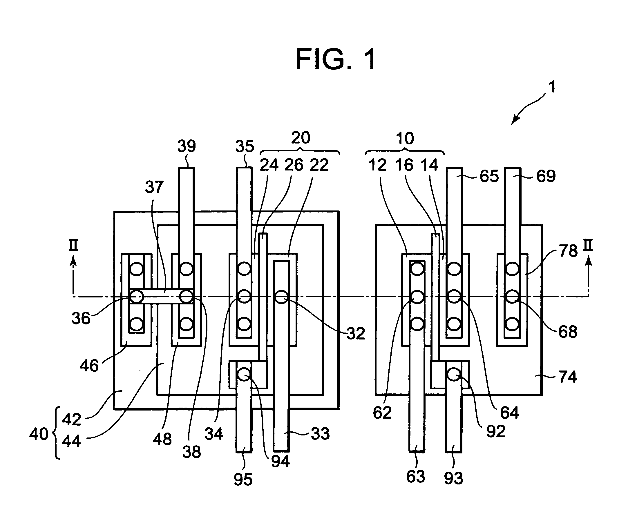
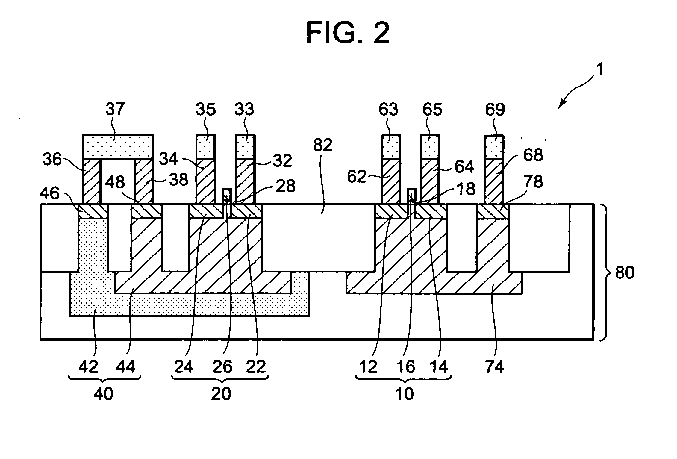
[0035]FIGS. 1 and 2 are a plan view and a sectional view, respectively, illustrating a first embodiment of a semiconductor memory device according to the present invention. FIG. 2 is a section taken along the line II-II of FIG. 1. FIG. 3 is a circuit diagram of the semiconductor memory device.

[0036]A semiconductor memory device 1 has a FET 10 (first field-effect transistor), a FET 20 (second field-effect transistor), a contact plug 32 (first conductive plug), contact plugs 34 (second conductive plugs), and a detection circuit 50. It is to be noted that, in FIGS. 1 and 2, the detection circuit 50 is omitted.

[0037]The FET 10 has an n+ diffusion layer 12 (source region), an n+ diffusion layer 14 (drain region), and a gate electrode 16. The gate electrode 16 is provided on a semiconductor substrate 80 with a gate insulating film 18 therebetween. In this embodiment, the semiconductor substrate 80 is a p-type silicon substrate. The FET 10 is formed in a p-type well region ...

Example

Second Embodiment

[0057]FIGS. 5 and 6 are a plan view and a section, respectively, illustrating a second embodiment of a semiconductor memory device according to the present invention. FIG. 6 is a section taken along the line VI-VI of FIG. 5. FIG. 7 is a circuit diagram of the semiconductor memory device. In a semiconductor memory device 2, both of the FET 10 and the FET 20 are provided in the same double well 40. Accordingly, the contact plugs 68, the wiring 69, and the diffusion layer 78 (see FIGS. 1 and 2) are not provided. Except for this, the structure of the semiconductor memory device 2 is the same as that of the semiconductor memory device 1. Further, the structure of a detection circuit 50 illustrated in FIG. 7 may be the same as that of the detection circuit 50 illustrated in FIG. 20.

[0058]Exemplary operation of the semiconductor memory device 2 is now described with reference to FIGS. 8A and 8B as a second embodiment of a method of writing data and a method of reading data...

Example

Third Embodiment

[0062]FIGS. 9 and 10 are a plan view and a sectional view, respectively, illustrating a third embodiment of a semiconductor memory device according to the present invention. FIG. 10 is a sectional view taken along the line X-X of FIG. 9. FIG. 11 is a circuit diagram of the semiconductor memory device. In a semiconductor memory device 3, the FET 10 and the FET 20 are provided in different double wells. Specifically, the FET 10 and the FET 20 are provided in the double well 40 and a double well 70, respectively. The double well 70 is formed by an n-type well region 72 (deep n-well) and the p-type well region 74. Contact plugs 66 are electrically connected to the well region 72 through an n+ diffusion layer 76. The contact plugs 66 and the contact plugs 68 are electrically connected to each other by wiring 67. Except for this, the structure of the semiconductor memory device 3 is the same as that of the semiconductor memory device 1.

[0063]It is to be noted that the pote...


PUM


Abstract

A semiconductor memory device (1) has a FET (10) (first field-effect transistor), a FET (20) (second field-effect transistor), a contact plug (32) (first conductive plug), contact plugs (34) (second conductive plugs), and a detection circuit (50). The FET (20) is provided in a double well (40). M (m is a natural number) contact plugs (32) are connected to a diffusion layer (22) of the FET (20) while n (n is a natural number) contact plugs (34) are connected to a diffusion layer (24). Here, m is smaller than n. The detection circuit (50) detects the difference between the output of the FET (10) and the output of the FET (20).

Description

BACKGROUND OF THE INVENTION[0001]1. Field of the Invention[0002]The present invention relates to a semiconductor memory device, a method of writing data therein, and a method of reading data therefrom.[0003]2. Description of the Related Art[0004]JP 2006-85753 A and JP 2006-338773 A each describe a conventional semiconductor memory device, for example. The semiconductor memory devices described in those documents each have a plurality of memory chips. Each memory chip has storing means where information for identifying the memory chip (chip ID) is stored. The storing means includes a plurality of fuses. The chip ID is adapted to be written by disconnecting / connecting the fuses. Specifically, whether the respective fuses have data of 0 or 1 is determined by whether the respective fuses are completely disconnected or not.[0005]It is to be noted that, in addition to JP 2006-85753 A and JP2006-338773A, JP2005-39220A is also given as the related art of the present invention.[0006]The pres...

Claims


Application Information

Patent Timeline
IPC IPC(8): G11C11/34G11C7/00
CPCG11C16/20G11C17/18H01L27/0207H01L27/0629H01L27/101H01L27/1021H01L27/112H01L27/11206H10B20/00H10B20/20
Inventor FUKAI, TOSHINORI
Owner RENESAS ELECTRONICS CORP
Why Eureka
Try Eureka