Atomic Layer Deposition Method and Semiconductor Device Formed by the Same

a technology of atomic layer and semiconductor, which is applied in the direction of semiconductor devices, chemical vapor deposition coatings, coatings, etc., can solve the problems of non-uniform size distribution of atomic islands, and achieve the effect of reducing current leakage, improving storage capability and memory isolation capability

Active Publication Date: 2008-12-25
SEMICON MFG INT (SHANGHAI) CORP
View PDF2 Cites 381 Cited by
  • Summary
  • Abstract
  • Description
  • Claims
  • Application Information

AI Technical Summary

Benefits of technology

[0021]The invention, compared with the prior art, has the following advantages:
[0022]1. The present invention provides an atomic layer deposition method, by which a first discrete compound monolayer is formed after forming a first discrete monolayer above a semiconductor substrate, and a first dielectric layer is formed on the first discrete compound monolayer, followed by forming a second discrete compound monolayer above the first dielectric layer, thereby forming one or more discrete compound monolayers above the semiconductor substrate and achieving a multi-layer discrete distribution of the atomic size nano-dots above the semiconductor substrate. Furthermore, with the ALD process, the sizes of the formed discrete compound monolayers are of precise atomic level and are uniform. The compound monolayers, when applied into the semiconductor device such as memory, can improve the storage capability and memory isolation capability, and decrease the current leakage.

Problems solved by technology

However, in the prior art, the charge trapping layer of discrete atomic islands (nano-dot) is generally formed by chemical vapor deposition or physical vapor deposition, and the size of the resulting atomic islands is in a range of 10 nm˜100 nm, and the size distribution of the atomic islands is non-uniform.

Method used


Image

  • Atomic Layer Deposition Method and Semiconductor Device Formed by the Same
  • Atomic Layer Deposition Method and Semiconductor Device Formed by the Same
  • Atomic Layer Deposition Method and Semiconductor Device Formed by the Same

Examples


first embodiment

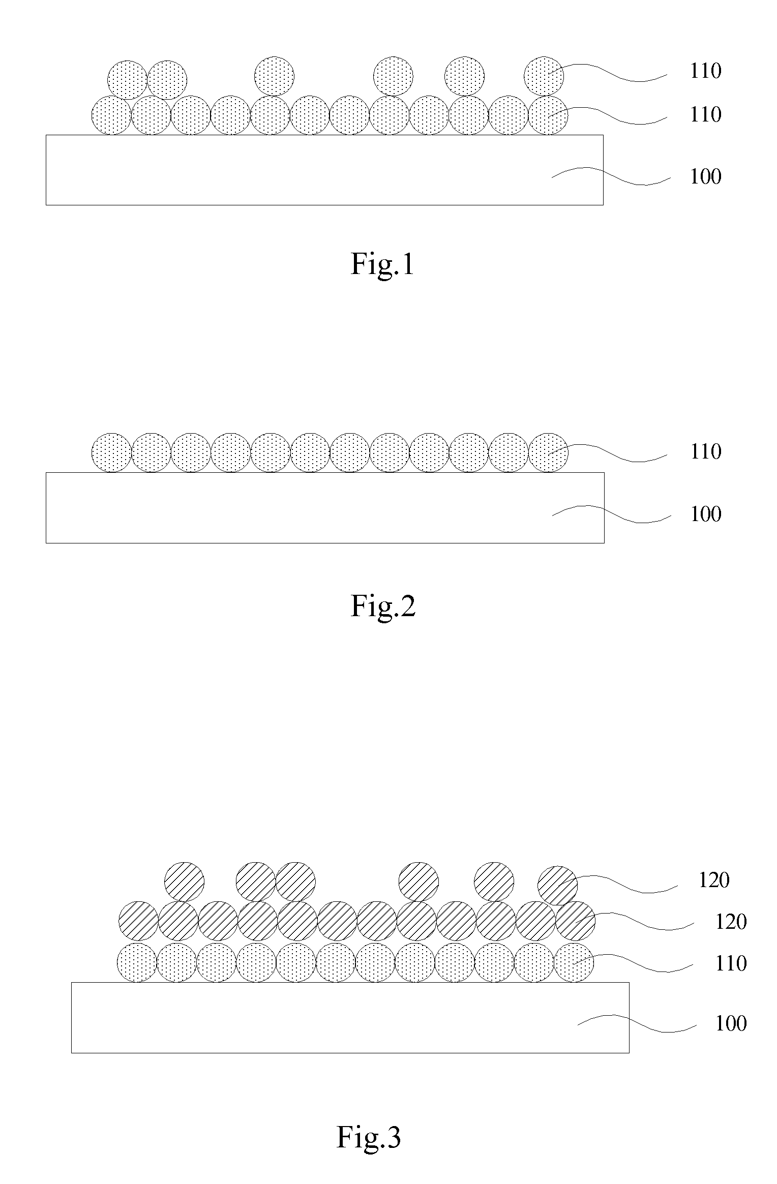
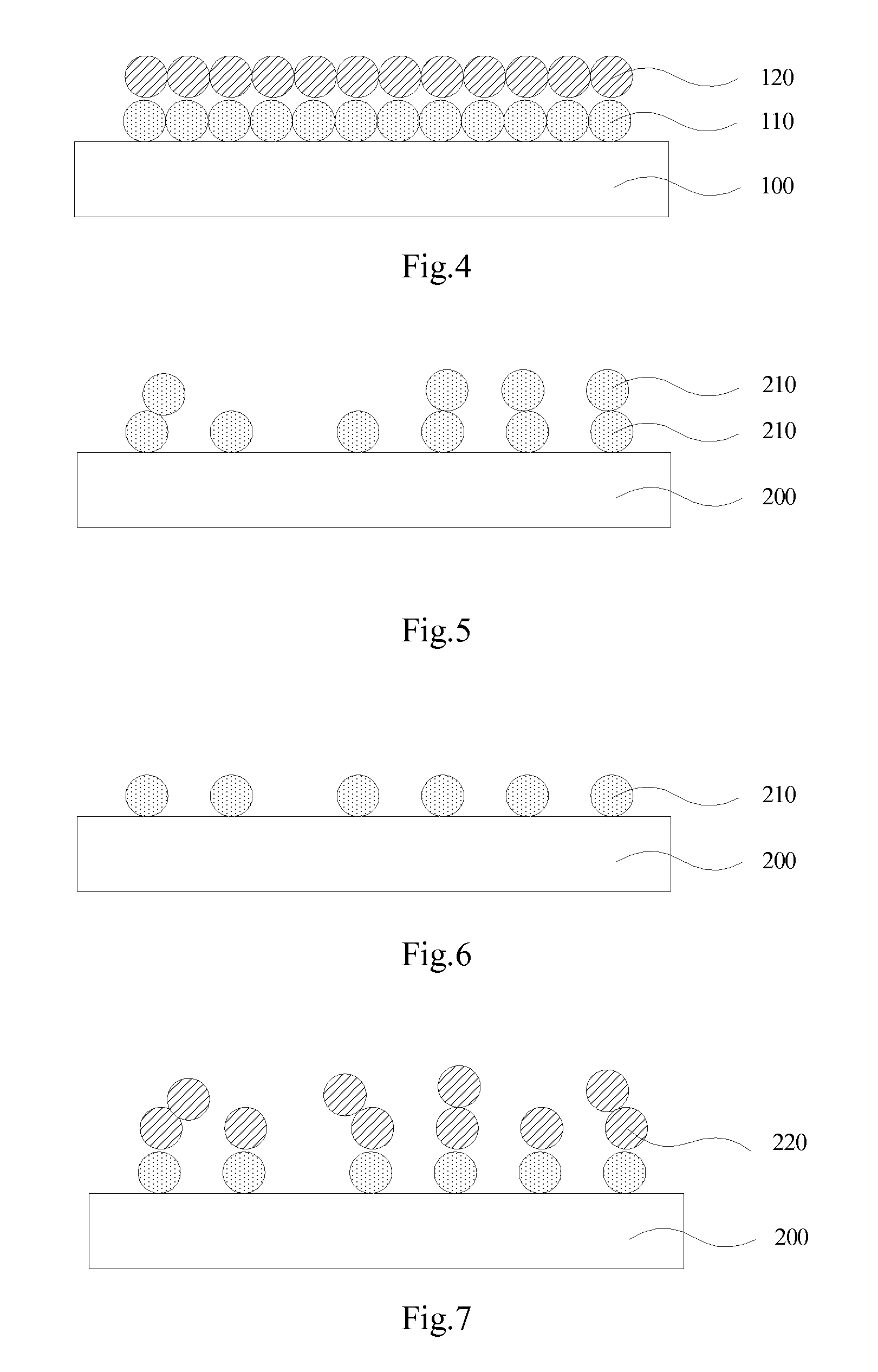
[0032]An atomic layer deposition method is provided in this embodiment. Referring to the flow diagram shown in FIG. 19, the method comprises the following steps: step S200, placing a semiconductor substrate in an atomic layer deposition chamber; step S201, flowing a first precursor gas to the semiconductor substrate within the atomic layer deposition chamber to form a first discrete monolayer on the semiconductor substrate; step S202, flowing an inert purge gas to the semiconductor substrate within the atomic layer deposition chamber to remove the first precursor gas which does not form the first monolayer on the semiconductor substrate; step S203, flowing a second precursor gas into the atomic layer deposition chamber to react with the first precursor gas which has formed the first monolayer to form a first discrete compound monolayer; step S204, flowing an inert purge gas into the deposition chamber to remove the second precursor gas that does not react with the first precursor ga...

second embodiment

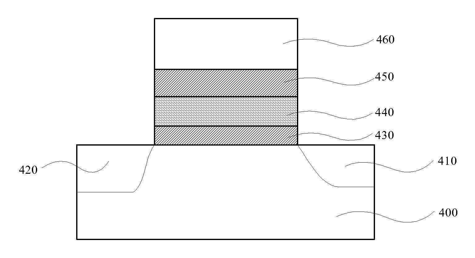
[0121]As shown in FIG. 20, there is provided a semiconductor device in this embodiment, comprising a semiconductor substrate 400, a three layer stack structure of medium layer 430—charge trapping layer 440—medium layer 450 arranged on the semiconductor substrate 400, and a gate 460 arranged on the three layer structure, and a source 410 and a drain 420 arranged in the semiconductor substrate at either side of the three layer structure, wherein the charge trapping layer 440 is a dielectric layer containing one or more discrete compound monolayers formed by atomic layer deposition. Here the word “containing” means that the one or more discrete compound monolayers are embedded in dielectric layers and covered by the same.

[0122]The semiconductor substrate 400 can include silicon(Si) or silicon germanium (SiGe) with monocrystal or polycrystal structure, ion-doped Si or SiGe such as N-doped or P-doped Si or SiGe, compound semiconductor such as silicon carbide, indium antimonide, lead tell...


PUM

PropertyMeasurementUnit
size distributionaaaaaaaaaa
temperatureaaaaaaaaaa

Abstract

There is provided a method of manufacturing a semiconductor device, including the following steps: flowing a first precursor gas to the semiconductor substrate within a ALD chamber to form a first discrete monolayer on the semiconductor substrate; flowing an inert purge gas to the semiconductor substrate within the ALD chamber; flowing a second precursor gas to the ALD chamber to react with the first precursor gas which has formed the first monolayer, thereby forming a first discrete compound monolayer; and flowing an inert purge gas; forming a first dielectric layer to cover the discrete compound monolayer; forming a second third monolayer above first dielectric layer; and forming a second discrete compound monolayer; and forming a second dielectric layer to cover the second discrete compound monolayer above the first dielectric layer. There is also provided a semiconductor device formed by the ALD method.

Description

FIELD OF THE INVENTION[0001]The present invention relates to a method for manufacturing a semiconductor, and more particularly, to an atomic layer deposition method and a semiconductor device manufactured by the same.DESCRIPTION OF THE RELATED ART[0002]Atomic layer deposition (ALD) is originally referred to as Atomic Layer Epitaxy (ALE), and is also termed as Atomic Layer Chemical Vapor Deposition (ALCVD).[0003]Atomic layer deposition involves the successive deposition of a plurality of monolayers over a semiconductor substrate within a deposition chamber typically maintained at a negative pressure (sub-atmospheric pressure). An exemplary method is disclosed in the background art of Chinese application No. 03818269, which comprising the following steps: feeding a first vaporized precursor into a deposition chamber to ly form a first monolayer 110 on the semiconductor substrate 100 placed in the deposition chamber, as shown in FIG. 1; thereafter, ceasing the flow of the first vaporiz...

Claims


Application Information

Patent Timeline
Patent Type & Authority Applications(United States)
IPC IPC(8): H01L21/28H01L29/792
CPCC23C16/45529H01L21/28282H01L29/1608H01L29/42348H01L29/792H01L29/40117
Inventor JI, HUACHI, MIN-HWAMIENO, FUMITAKEZHANG, SEANFUXIONG
Owner SEMICON MFG INT (SHANGHAI) CORP
Why Eureka
Try Eureka