Packaging substrate with embedded chip and buried heatsink

a technology of embedded chips and heatsinks, which is applied in the manufacture of printed circuits, printed circuit aspects, basic electric elements, etc., can solve the problems of large chip package designers, large chip package sizes, and large chip package sizes, and achieve the effect of improving the embedded chip package structure and increasing the use of the substra

Inactive Publication Date: 2008-12-25
NAN YA PRINTED CIRCUIT BOARD CORPORATION
View PDF2 Cites 104 Cited by
  • Summary
  • Abstract
  • Description
  • Claims
  • Application Information

AI Technical Summary

Benefits of technology

[0010]It is another object of the present invention to provide an improved embedded chip package structure, wherein various components such as active or passive components may be embedded in the substrate to increase the usage of the substrate and to make the package lighter and thinner to meet the future trends.

Problems solved by technology

For chip packages, electrical performance and dissipation control are two major challenges.
In addition to electrical performance and dissipation control, the small size of the microcontroller also demands smaller chip package size and denser I / O pad arrangements.
In the future, a chip package may comprise several dies and opto-electronic elements, and minimizing the space between elements, maximizing the interconnectivity of elements, controlling signal frequency precisely, and matching impedance will be great issues for chip package designers.
In conclusion, the prior art package technology, such as FCPGA, will not satisfy new requirements.
However, defects often occur during the process of routing wires on the surface layers.
This problem decreases product quality, and increases the product cost so that the BBUL package may cost much more than the conventional package method.
Furthermore, because of the difference in the coefficients of thermal expansion of the die, the underfill and the substrate, cracks may occur during the routing process.
Moreover, the heat dissipation performance also needs to be improved in the conventional BBUL package, so there are still a lot of problems to be solved in the conventional BBUL package.

Method used


Image

  • Packaging substrate with embedded chip and buried heatsink
  • Packaging substrate with embedded chip and buried heatsink
  • Packaging substrate with embedded chip and buried heatsink

Examples


Embodiment Construction

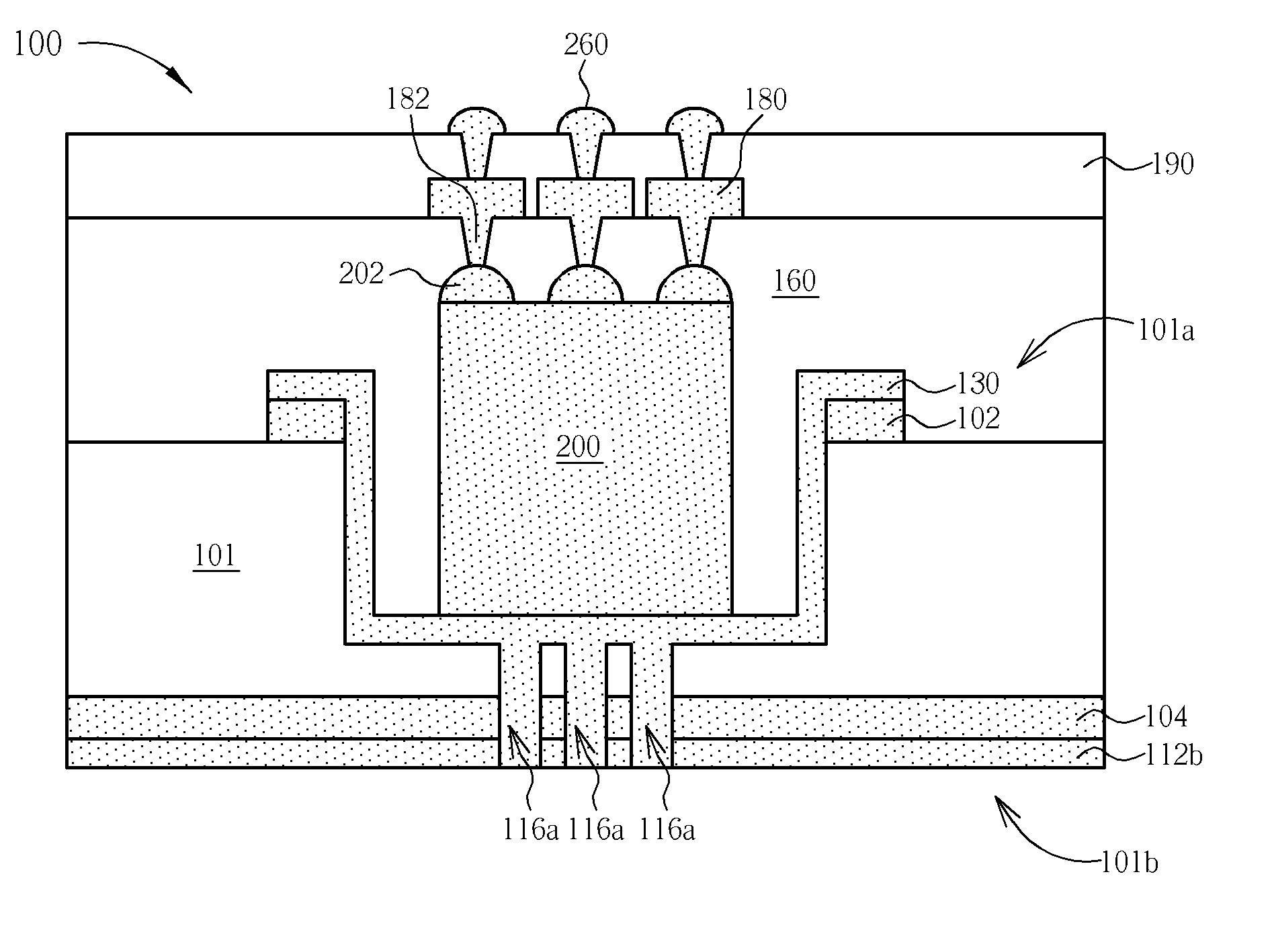
[0016]Please refer to FIGS. 1-14. FIGS. 1-14 are schematic, cross-sectional diagrams illustrating a method for fabricating an embedded chip package in accordance with the preferred embodiment of this invention.

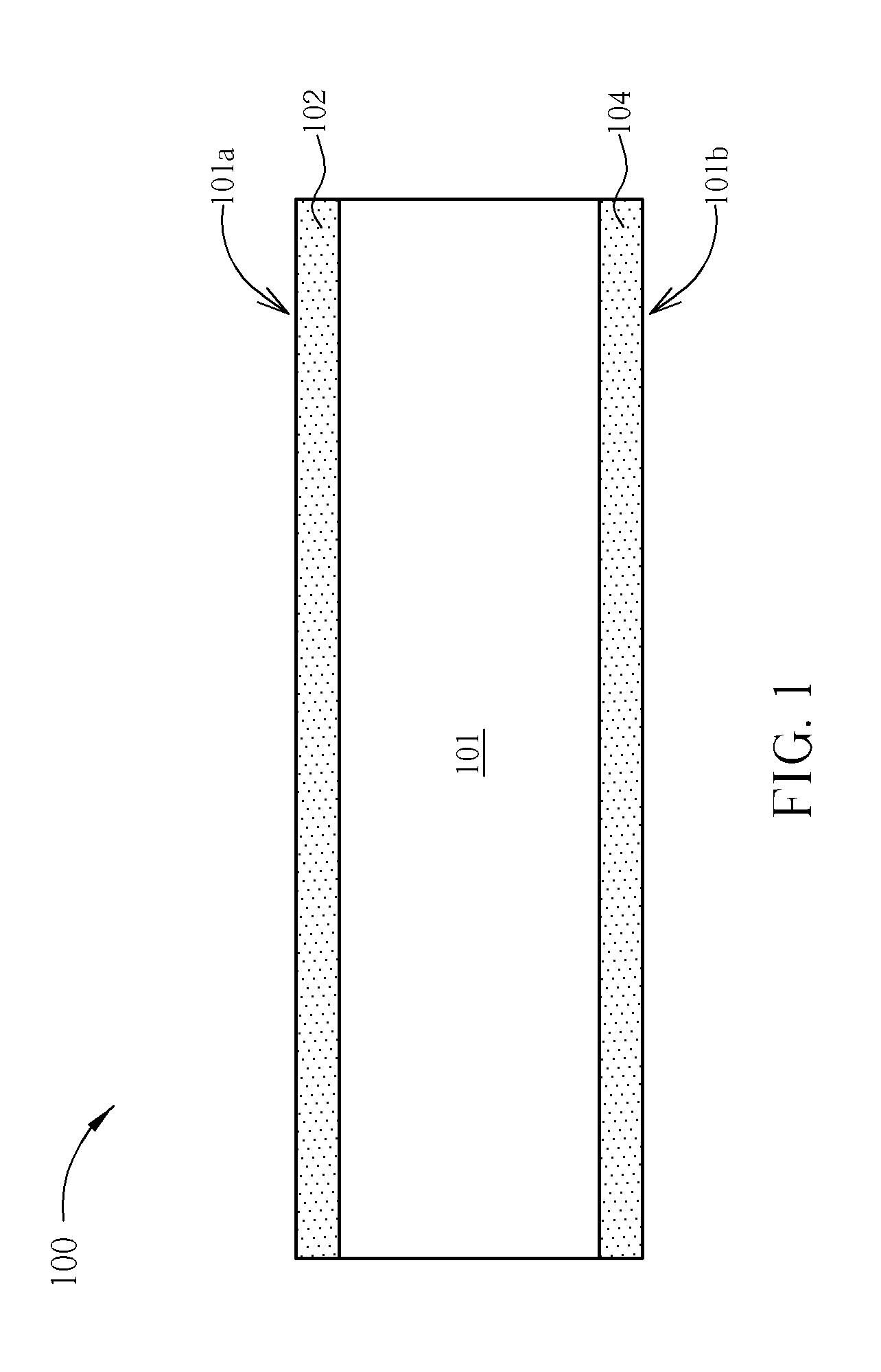
[0017]As shown in FIG. 1, a substrate 100, such as double-sided copper clad laminate (CCL), is provided, which comprises a dielectric interposer 101, a first metal foil 102 positioned on a first surface 101a of the substrate 100, and a second metal foil 104 positioned on a second surface 101b of the substrate 100.

[0018]The dielectric interposer 101 may be made of glass fiber or resins. The first metal foil 102 and the second metal foil 104 may be composed of copper, iron, gold or aluminum, preferably copper. Generally, the thickness of the present invention embedded chip substrate is not critical. However, a preferable substrate thickness is less than 800 micrometers.

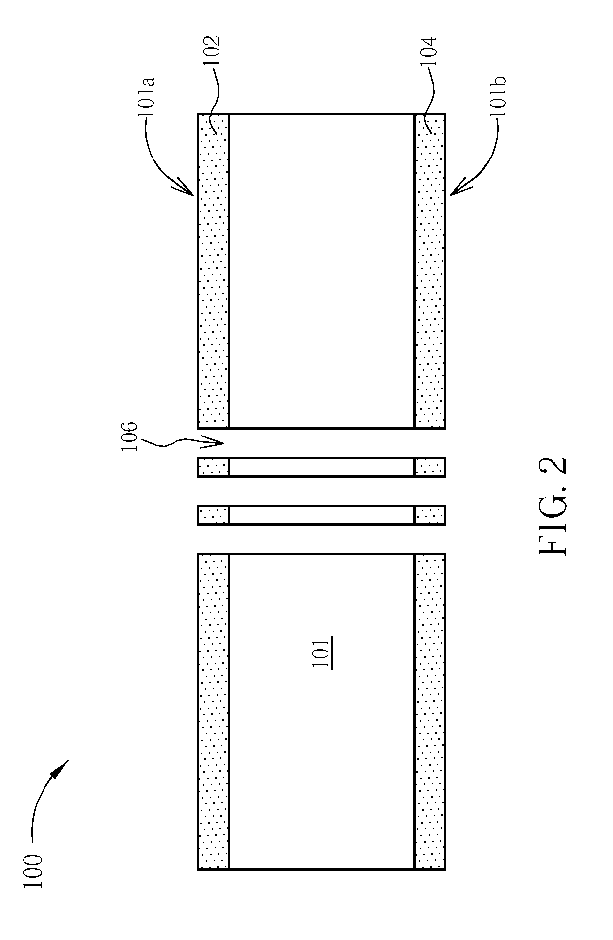
[0019]As shown in FIG. 2, a drilling process such as laser drilling or mechanical drilling is carried out to fo...


PUM

PropertyMeasurementUnit
thicknessaaaaaaaaaa
dielectricaaaaaaaaaa
heat-dissipatingaaaaaaaaaa

Abstract

An embedded chip package includes a substrate having a dielectric interposer, a first metal foil on a first surface and a second metal foil on a second surface of the substrate, wherein the substrate has a cavity recessed into the first surface; a metal heatsink embedded within the cavity; a semiconductor die mounted on a flat bottom of the metal heatsink; a dielectric layer covering the first surface of the substrate; at least one built-up circuit trace layer on the dielectric layer; a solder resist layer on the built-up circuit trace layer and on the dielectric layer; a heat-dissipating metal layer on the second metal foil; and heat-dissipating plugs connecting the flat bottom of the metal heatsink and the heat-dissipating metal layer.

Description

BACKGROUND OF THE INVENTION[0001]1. Field of the Invention[0002]The present invention relates to packaging substrates, and more particularly to an embedded chip package and packaging substrate thereof with improved heat dissipation performance.[0003]2. Description of the Prior Art[0004]With the rapid development of electronic technology, the number of I / O pads in microcontrollers is drastically increasing, and the power that each silicon chip consumes has also increased. In the future, microcontrollers may have more pins. For chip packages, electrical performance and dissipation control are two major challenges. In the aspect of electrical performance, chip packages have to maintain integrity of signals and operating frequency of semiconductor devices. In the aspect of dissipation control, chip packages also help dissipate heat generated by the silicon chip.[0005]In addition to electrical performance and dissipation control, the small size of the microcontroller also demands smaller...

Claims


Application Information

Patent Timeline
Patent Type & Authority Applications(United States)
IPC IPC(8): H01L23/48H01L23/10
CPCH01L23/3675H01L23/3677H01L23/5389H01L24/24H01L24/82H01L2224/24227H01L2224/82039H01L2224/82047H01L2924/01013H01L2924/01029H01L2924/01078H01L2924/01079H01L2924/15311H01L2924/3011H05K1/0206H05K1/183H05K1/185H05K3/4644H05K2201/09981H05K2201/10674H01L2924/01033H01L2924/01047H01L2924/014H01L24/19H01L2924/10253H01L2924/00H01L2224/12105H01L2224/73267H01L2924/00011H01L2924/00014H01L2924/15153H01L2224/0401
Inventor LO, HSING-LUNLIN, SHIH-TSUNGLIN, HSIEN-CHIEHCHIANG, KUO-CHUN
Owner NAN YA PRINTED CIRCUIT BOARD CORPORATION
Why Eureka
Try Eureka