Thin Film Transistor and Display Device, and Method for Manufacturing Thereof

a technology of thin film transistors and display devices, which is applied in the direction of instruments, conductive pattern formation, coatings, etc., can solve the problems of increasing manufacturing costs, reducing the number of processes, and affecting the appearance of large substrates having a side of 1 meter or more, so as to reduce costs, reduce material loss, and control the effect of well

Inactive Publication Date: 2008-12-25
SEMICON ENERGY LAB CO LTD
View PDF3 Cites 29 Cited by
  • Summary
  • Abstract
  • Description
  • Claims
  • Application Information

AI Technical Summary

Benefits of technology

[0292]As explained in Embodiment 1, a mask is formed in a subject formation region. As a mask, polyimide is used. The polyimide is discharged over a substrate by droplet discharging. The substrate is formed to have low wettability by using a low wettability substance. FAS is used as the low wettability substance and diluted by octanol of solvent to be coated. Thereafter, the mask is removed. According to the foregoing processes, a low wettability region and a high wettability region are formed, and so the subject formation region has different level of wettability.
[0293]A silver wiring is formed by discharging a composition containing a silver conductive material by droplet discharging so as to be crossed a boundary between the high wettability region and the low wettability region. A dot pitch for drawing is 60 μm. The dot pitch is a distance between dots. The composition containing silver discharged over the region of low wettability does not settle in there due to the difference of wettability of the subject formation region, and partly flows into the high wettability region from the boundary between the high wettability region and the low wettability region. This arises from the fact that the composition containing silver is repelled in the low wettability region that has low wettability with respect to the composition containing silver, and so the composition does not fix thereto, and flows to the high wettability region having further high stability. As a result, as shown in FIG. 40, the silver wiring formed over the low wettability region is formed with stability into a fine wiring to have a thickness of 400 nm, a width of from 50 to 55 μm, and a length of 1 mm. Therefore, a fine wiring can be freely formed according to the present invention.
[0294]As a comparative example, an example of forming a silver wiring in accordance with the foregoing ways without using the present invention is described. A whole subject formation region is formed to have low wettability. Accordingly, the subject formation region has uniform wettability. A silver wiring is formed by discharging a silver conductive material over the region having uniform wettability. FIGS. 41A and 41B show the results. The silver wirings illustrated in FIGS. 41A and 41B are formed by discharging different amounts of materials; FIG. 41A shows a wiring formed with a dot pitch of 60 μn, and FIG. 41B shows a wiring formed with a dot pitch of 50 μm.
[0295]In the comparative example, breaking is produced as illustrated in FIG. 41A in the silver wiring formed with a dot pitch of 60 μm, with which the silver wiring with stability can be formed in this embodiment. Breaking is not produced in the silver wiring having a dot pitch of 50 μm formed by a large discharge rate, in turn, swelling referred to as bulge due to a puddle of liquid is produced therein. The wiring according to the comparative example is formed to have a thickness of 900 nm. Therefore, the wirings formed according to the comparative example have shape deterioration due to breaking or stagnant liquid that does not use the present invention. A stable fine wiring cannot be formed according to the comparative example.
[0296]As noted above, it can be confirmed that a stable fine pattern can be formed according to the present invention.EXAMPLE 2
[0297]An example of a pattern according to the present invention is explained based on experimental results in this example 2.

Problems solved by technology

Therefore, the increase of the number of the photolithography processes inevitably leads to the increase of a manufacturing cost.
However, the technique disclosed by Unexamined Patent Publication No. 11-251259 does not contribute to reduce drastically the number of processes, since a part of the photolithography processes performed at a plurality of times in a TFT manufacturing process is merely substituted by a printing process.
In principle, it is technically-difficult that a large substrate having a side of 1 meter or more is exposed at one time by the photolithography machine.

Method used


Image

  • Thin Film Transistor and Display Device, and Method for Manufacturing Thereof
  • Thin Film Transistor and Display Device, and Method for Manufacturing Thereof
  • Thin Film Transistor and Display Device, and Method for Manufacturing Thereof

Examples


embodiment 1

[0069]Although the present invention will be fully described by way of embodiments with reference to the accompanying drawings, it is to be understood that various changes and modifications will be apparent to those skilled in the art. Therefore, unless otherwise such changes and modifications depart from the scope of the present invention hereinafter described, they should be construed as being included therein. Through the drawing of the embodiments, same components are denoted by same numerals, and will not be further explained.

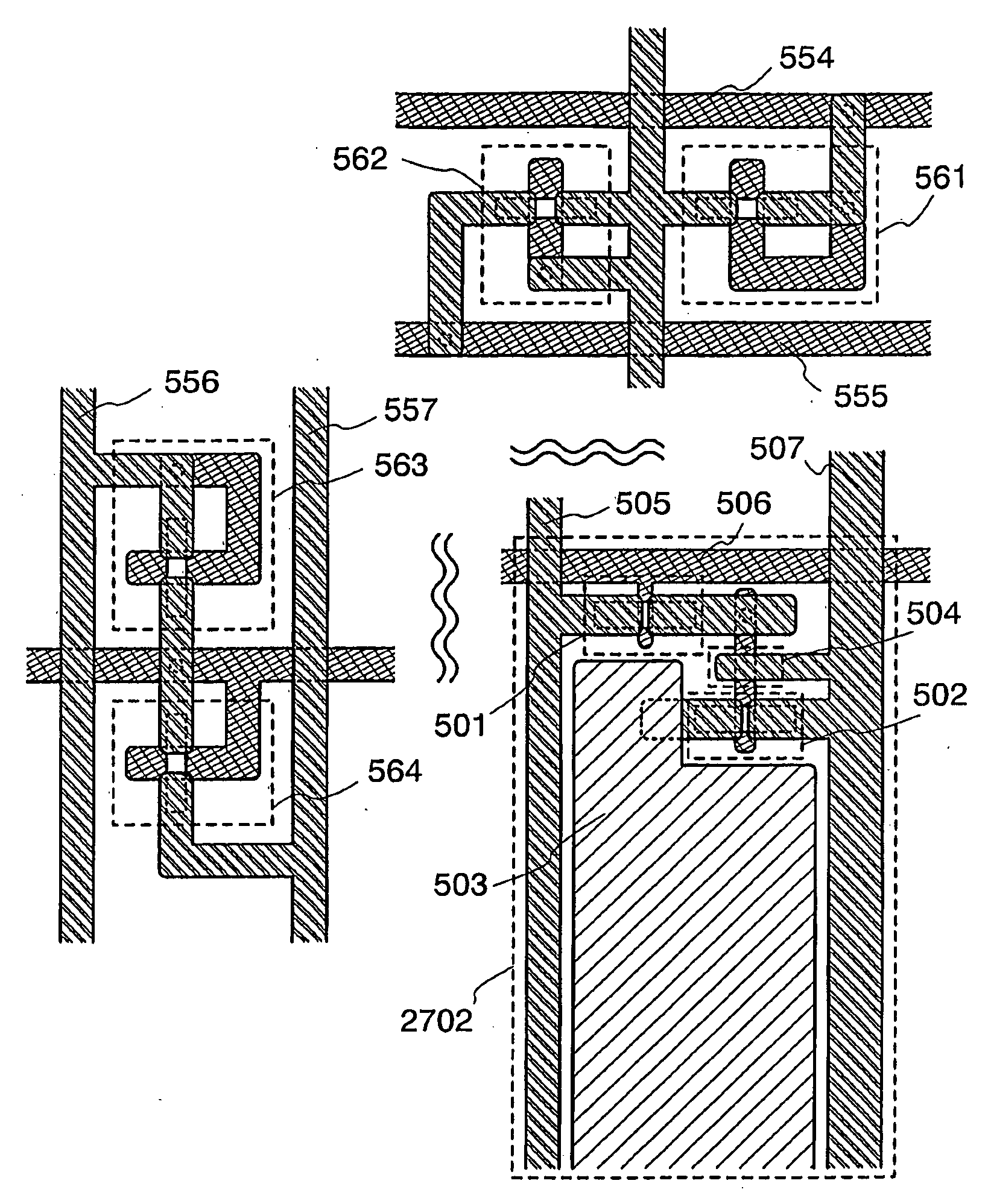
[0070]FIG. 29A illustrates a top view for showing an example of a structure of a display panel according to the present invention. A pixel portion 2701 composed of pixels 2702 in a matrix configuration over a substrate 2700 having an insulating surface, a scanning line side input terminal 2703, and a signal line side input terminal 2704 are formed. The number of pixels may be set according to various specifications, for example, 1024×768×3 (RGB) for XGA, 1...

embodiment 2

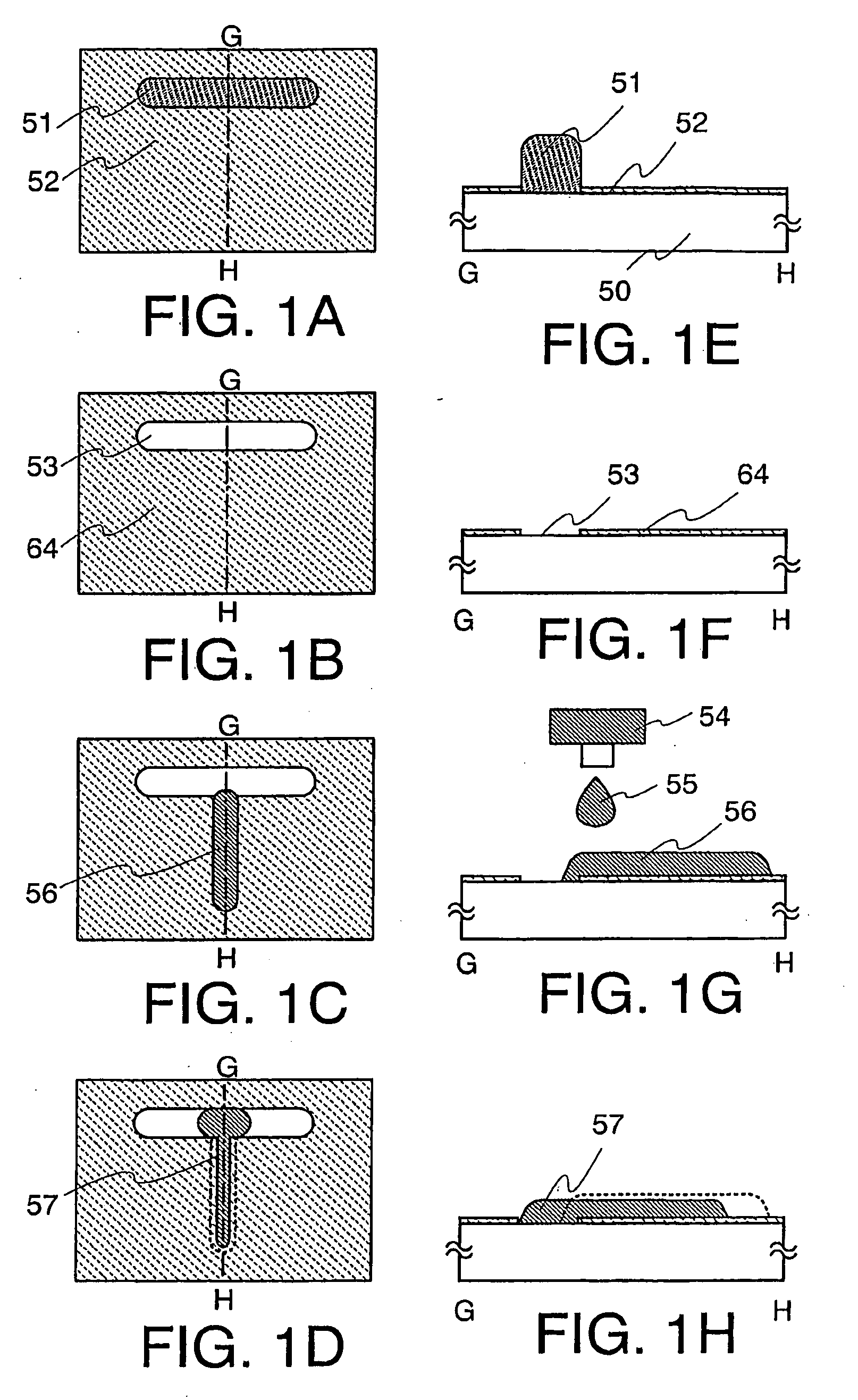
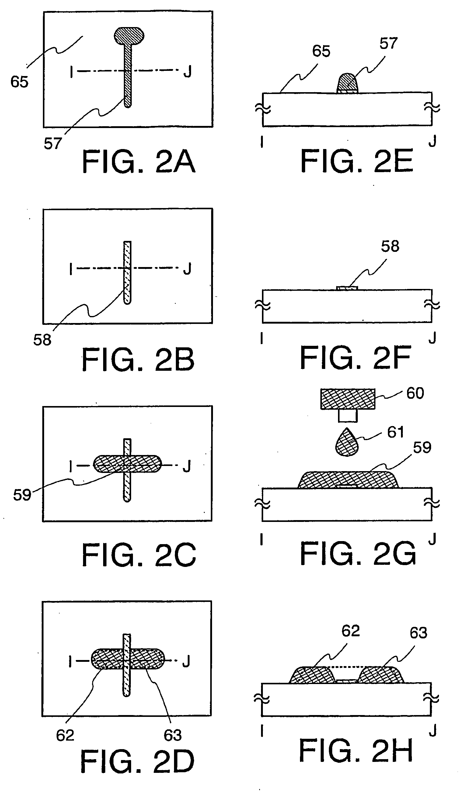
[0102]An embodiment of the present invention is explained with reference to FIGS. 2A to 2H. FIGS. 2A to 2D are top views of a pattern. FIGS. 2E to 2H are cross-sectional views taken along line I-J of FIGS. 2A to 2D. FIG. 2A to 2D correspond respectively to FIGS. 2E to 2H.

[0103]In this embodiment, another example of forming a pattern according to the present invention is explained. In Embodiment 1, an example of forming a pattern into a fine line is explained. In this embodiment, an example of forming finely spaced apart patterns with good controllability is explained.

[0104]FIG. 2A illustrates the state that a low wettability substance 52 that has an effect of imparting low wettability is removed from the state illustrated in FIG. 1D using a pattern 57 as a mask. As illustrated in FIG. 2E, only the low wettability substance 52 is left below the pattern 57 and the periphery thereof is a high wettability region 65. The high wettability region has high wettability since it has not the l...

embodiment 3

[0107]This embodiment is explained with reference to FIGS. 38A to 38D. FIGS. 38A to 38D illustrates a top view of a pattern.

[0108]This embodiment shows an example of forming a pattern formed to be a fine line in Embodiment 1 is formed further longer to form a fine and long pattern.

[0109]A plurality of masks 71a, 71b, and 71c are provided spaced apart over a substrate 70. Thereafter, a low wettability substance 72 is formed by using the masks 71a, 71b, and 71c (FIG. 38A). Then, the masks 71a, 71b, and 71c are removed by etching. A low wettability region 78, and high wettability regions 73a, 73b, and 73c are selectively formed over the substrate 70 (FIG. 38B).

[0110]A droplet of a composition containing a pattern formation material having fluidity is discharged so as to be crossed the high wettability regions 73a, 73b, and 73c and to be straddled the low wettability region by droplet discharging. The composition containing a pattern formation material is discharged from a nozzle as a d...


PUM

PropertyMeasurementUnit
grain diametersaaaaaaaaaa
contact angleaaaaaaaaaa

Abstract

The present invention discloses a display device and a manufacturing method thereof by which a manufacturing process can be simplified. Further, the present invention discloses technique for manufacturing a pattern such as a wiring into a desired shape with good controllability. A method for forming a pattern for constituting the display device according to the present invention comprises the steps of forming a first region and a second region; discharging a composition containing a pattern formation material to a region across the second region and the first region; and flowing a part of the composition discharged to the first region into the second region; wherein wettability with respect to the composition of the first region is lower than that of the second composition.

Description

TECHNICAL FIELD[0001]The present invention relates to a method for forming a pattern, a thin film transistor, a method for manufacturing the same, a display device, a method for manufacturing the same, and a television device using the foregoing thin film transistor and display device.BACKGROUND ART[0002]A thin film transistor (hereinafter, TFT) and an electronic circuit using the TFT is manufactured by stacking various thin films such as a semiconductor, an insulator, or a conductor over a substrate, and forming appropriately a predetermined pattern by photolithography technique. The photolithography technique means technique of transferring a pattern such as a circuit made from a material that does not transmit light formed over a transparent plane surface referred to as a photomask to a substrate by utilizing light. The photolithography technique is widely used in a manufacturing process for a semiconductor integrated circuit and the like.[0003]In a manufacturing process using th...

Claims


Application Information

Patent Timeline
Patent Type & Authority Applications(United States)
IPC IPC(8): H01L21/768H01L23/535B05D1/26G02F1/1362H01L21/28H01L21/288H01L21/3205H01L21/336H01L21/77H01L21/84H01L29/786H05K3/12
CPCG02F2001/136295H01L21/288H01L27/1292H05K3/1241H01L27/1285H01L29/66742G02F1/136295H01L27/1214H01L27/124H01L29/4908
Inventor FUJII, GEN
Owner SEMICON ENERGY LAB CO LTD
Why Eureka
Try Eureka