Nonvolatile semiconductor memory device

a semiconductor memory and non-volatile technology, applied in information storage, static storage, digital storage, etc., can solve the problems of increased access time or occurrence of erroneous reading, inaccurate reading, and inability to quickly change the read current, etc., to achieve high reliability

Inactive Publication Date: 2008-12-25
RENESAS TECH CORP
View PDF7 Cites 46 Cited by
  • Summary
  • Abstract
  • Description
  • Claims
  • Application Information

AI Technical Summary

Benefits of technology

[0018]An object of the present invention is to provide a nonvolatile semiconductor memory device that can write and read data with high reliability.
[0019]Another object of the present invention is to provide a phase change memory that can achieve fast data reading.
[0025]In the nonvolatile semiconductor memory device according to the first aspect, the reference cell is formed of the memory element in the state other than the state corresponding to the first resistance state. Therefore, even when the read current flows through the reference cell more times than the normal memory cell, the possibility that the state of the reference cell changes is small. Thus, the read disturbance can be prevented, and the reference current can be accurately produced.
[0026]In the nonvolatile semiconductor memory device according to the second aspect, memory cells are arranged so as for each source line to be connected to the selected memory cell of one bit in the data write operation. Thus, the write current merely flows to the source line through the one selected memory cell. Therefore, the mutual interference of the write currents between the selected memory cells can be prevented, and fast and accurate data writing can be achieved. By configuring the write current path each to have the resistance value not greater than 500Ω, the voltage applied to the memory cell is 2 V even when the power supply voltage is 3 V, and therefore a sufficiently large current can be supplied to the memory cell, so that the data writing can be reliably performed even under a low power supply voltage condition.
[0027]According to the nonvolatile semiconductor memory device of the third aspect, the path of the write current routing from the write current source through the data line, the bit line and the source line, excluding memory cells is formed to have the total resistance value substantially constant independently of the position of a selected address, and it is possible to suppress dependency of the write current on the position of the selected memory cell in the array, so that accurate writing can be performed, and the write margin can be increased.

Problems solved by technology

When the source line is shared between the memory cells from which the data are concurrently read, read currents flow in parallel through these selected memory cells, and may cause mutual interference between the selected memory cells through the shared source line, so that accurate reading may be difficult.
When the large current raises the source line potential, the raised potential restricts the read currents of the other selected memory cells, which causes a problem of increase in access time or occurrence of erroneous reading.
Accordingly, a read current path is associated with a stray capacitance of write circuitry for supplying the large write current, resulting in a problem that read current can not be changed fast.
In this construction, however, two variable resistance elements store data of one bit, so that a storage capacity is small.
Since the read current flows through the reference cell, this read current may cause read disturbance, that the state of the phase change material element slowly changes from the amorphous state to the crystalline state, leading to a problem that an accurate reference current cannot be produced.
Consequently, a problem arises that a margin for the sense operation in data reading lowers, and accordingly, fast reading of accurate data cannot be achieved.
In this case, therefore, when the lengths of the internal data line, bit line and source line included in the write current path change depending on the selected address position, the total resistance value of the write current path changes to change the write current value, which results in a problem that a margin in the data write operation is impaired and data writing cannot be performed fast.
For example, a large write current flows to the shared source line via the memory cell of the smallest resistance value, to raise the potential on the shared source line to restrict the write currents of other memory cells, resulting in an erroneous data writing or others.
Further, the write current needs to be large, but a sufficiently large write current cannot flow due to the electric resistance of the shared source line, which may cause erroneous writing.

Method used


Image

  • Nonvolatile semiconductor memory device
  • Nonvolatile semiconductor memory device
  • Nonvolatile semiconductor memory device

Examples


first embodiment

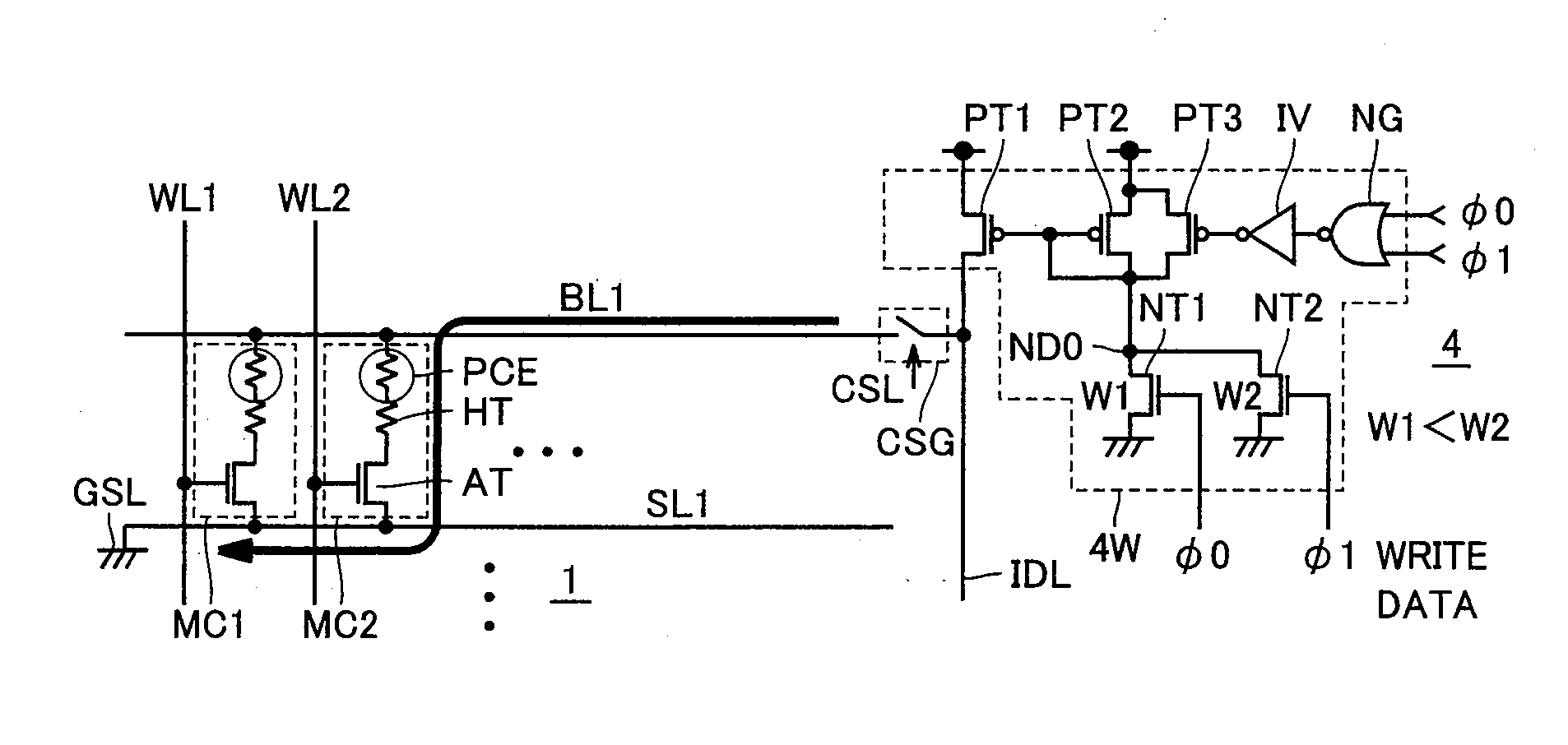
[0098]FIG. 1 schematically shows a configuration of a main portion of a nonvolatile semiconductor memory device according to a first embodiment of the invention. In FIG. 1, a nonvolatile semiconductor memory device includes a memory cell array 1 having memory cells MC arranged in rows and columns. In memory cell array 1, word lines WL are arranged corresponding to the respective rows of memory cells MC, and bit lines BL are arranged corresponding to the respective memory cell columns. Source lines SL are provided corresponding to and in parallel to bit lines BL, respectively. Source lines SL are coupled to a global source line GSL that extends along a first side of memory cell array 1 perpendicularly to bit line BL and source line SL. Global source line GSL is coupled to a ground node (ground pad; reference potential source). Memory cell MC, of which structure will be described later, includes a phase change material element as a storage element, and the phase change material elemen...

second embodiment

[0161]FIG. 12 shows a construction of an array portion of a nonvolatile semiconductor memory device according to a second embodiment of the invention. In FIG. 12, bit lines BL1-BL4 are arranged, and source line SL1 is arranged corresponding to and between bit lines BL1 and BL2, in parallel to them. Source line SL2 is arranged corresponding to and between bit lines BL3 and BL4, in parallel to them. Bit lines BL1-BL4 are coupled to an internal write data line WDB included in internal data line IDL via column select gates CSG1-CSG4, respectively.

[0162]Source lines SL1 and SL2 are commonly connected to global source line GSL. Memory cells MC11, MC12, . . . are connected to bit line BL1, memory cells MC21, MC22, . . . are connected to bit line BL2, memory cells MC31, MC32, . . . are connected to bit line BL3 and memory cells MC41, MC42, . . . are connected to bit line BL4.

[0163]Source line SL1 is shared between the memory cells connected to bit line BL1 and BL2. Thus, access transistors ...

third embodiment

[0285]FIG. 39 schematically shows a construction of a main portion of a nonvolatile semiconductor memory device according to a third embodiment of the invention. In FIG. 39, the nonvolatile semiconductor memory device includes, similarly to the first embodiment, memory cell array 1 having memory cells MC arranged in rows and columns, row select circuit 2 for driving a word line corresponding to the selected row in memory cell array 1 to the selected state, column select circuit 3 for producing a column select signal for a selected column in memory cell array 1 according to an address signal (not shown), and connecting the selected column to write data line WDB according to the column select signal, and write / read circuit 4 including variable current source 4W supplying the write current to write data line WDB in the data write operation.

[0286]In memory cell array 1, bit line BL is arranged corresponding to each column of memory cells MC, and word line WL is arranged corresponding to...


PUM


Abstract

A path routing from a write current source supplying a write current through an internal data line, a bit line and a source line to a reference potential except a memory cell is configured to have a constant resistance independent of a memory cell position selected in a memory array, and each of the resistance value of the current path between the memory cell and the write current source and the resistance value of the current path between the selected memory cell and the reference potential node is set to 500Ω or lower. A nonvolatile semiconductor memory device having improved reliability of data read / write is achieved.

Description

BACKGROUND OF THE INVENTION[0001]1. Field of the Invention[0002]The present invention relates to a nonvolatile semiconductor memory device, and particularly to a construction for improving reliability of write and read data of a phase change memory including memory cells each having a data storing element which selectively attains a crystalline state (polycrystalline state) and an amorphous state in accordance with stored data.[0003]2. Description of the Background Art[0004]Nonvolatile memories storing information in a nonvolatile manner have been widely employed in application of portable equipment and others. As such nonvolatile memories, there are a flash memory storing information by storing charges on a floating gate of a stacked gate transistor, and a memory utilizing a resistance value change type memory cell having a resistance value of a memory element changed according to stored information. As the resistance value change type memories, there are known various memories suc...

Claims


Application Information

Patent Timeline
Patent Type & Authority Applications(United States)
IPC IPC(8): G11C11/00G11C7/00G11C8/00
CPCG11C11/56G11C11/5678G11C13/0004G11C13/003G11C13/004G11C13/0069G11C2013/0054G11C2213/75G11C2213/76G11C2213/79G11C13/02
Inventor TANIZAKI, HIROAKIHIDAKA, HIDETO
Owner RENESAS TECH CORP
Why Eureka
Try Eureka