

Crosslinkable Graft Polymer Non-Preferentially Wetted by Polystyrene and Polyethylene Oxide
- Summary
- Abstract
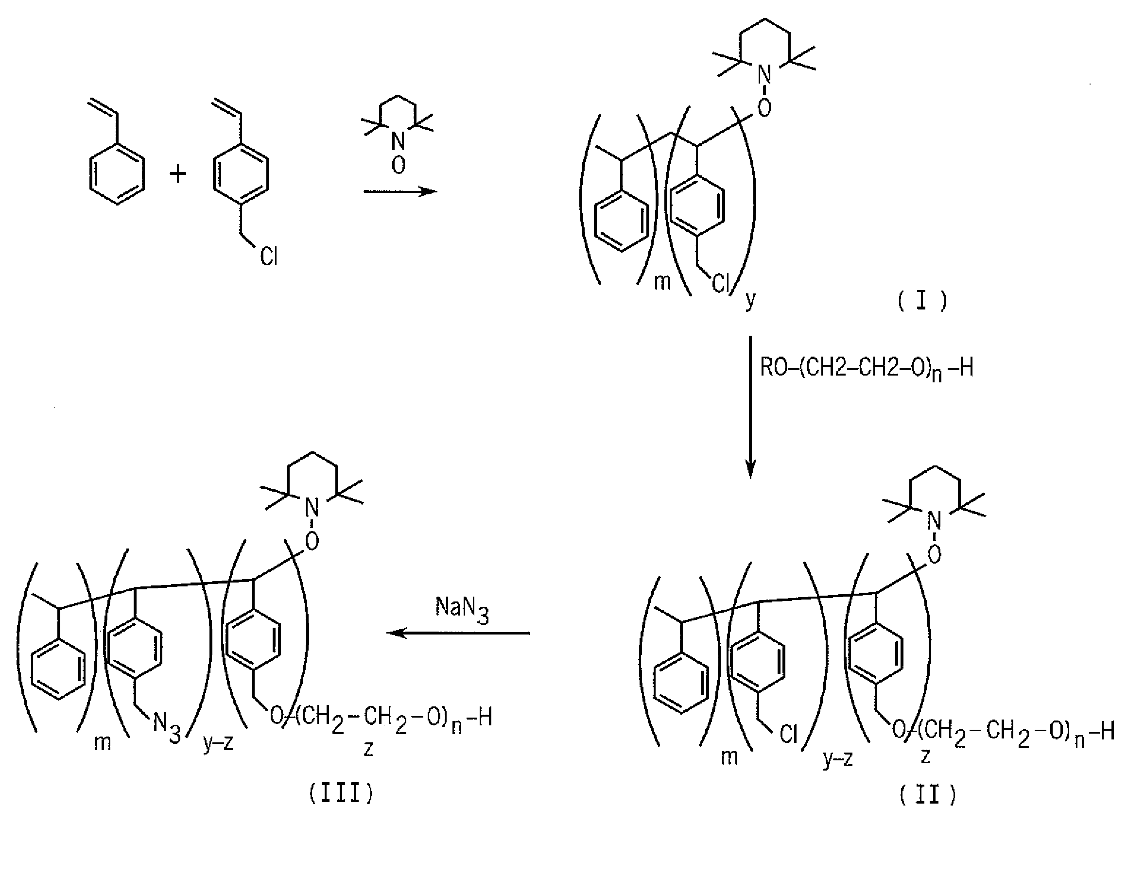
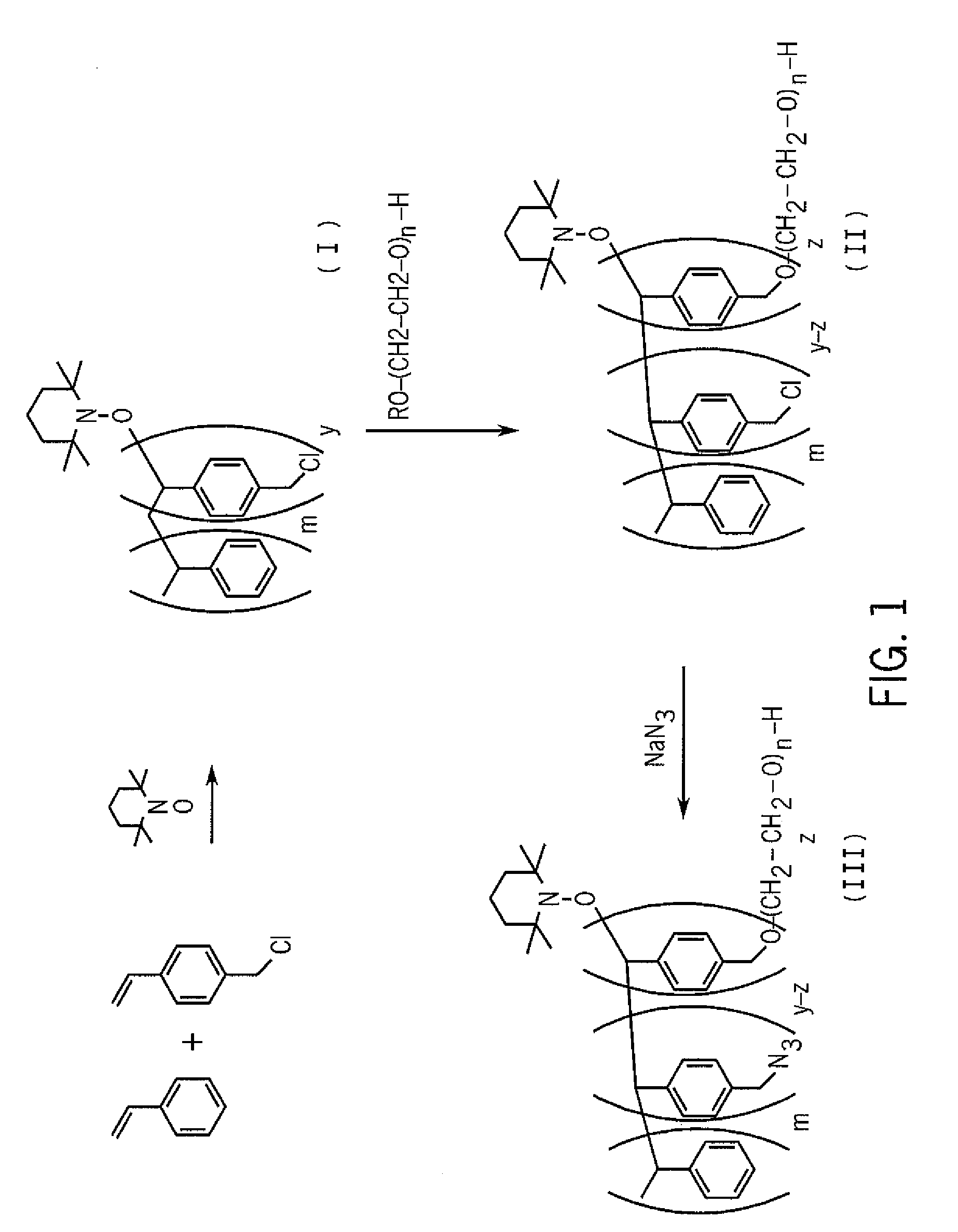
- Description
- Claims
- Application Information
AI Technical Summary
Problems solved by technology
Method used
Image

Examples
Embodiment Construction
[0022]The following description with reference to the drawings provides illustrative examples of devices and methods according to embodiments of the invention, Such description is for illustrative purposes only and not for purposes of limiting the same.
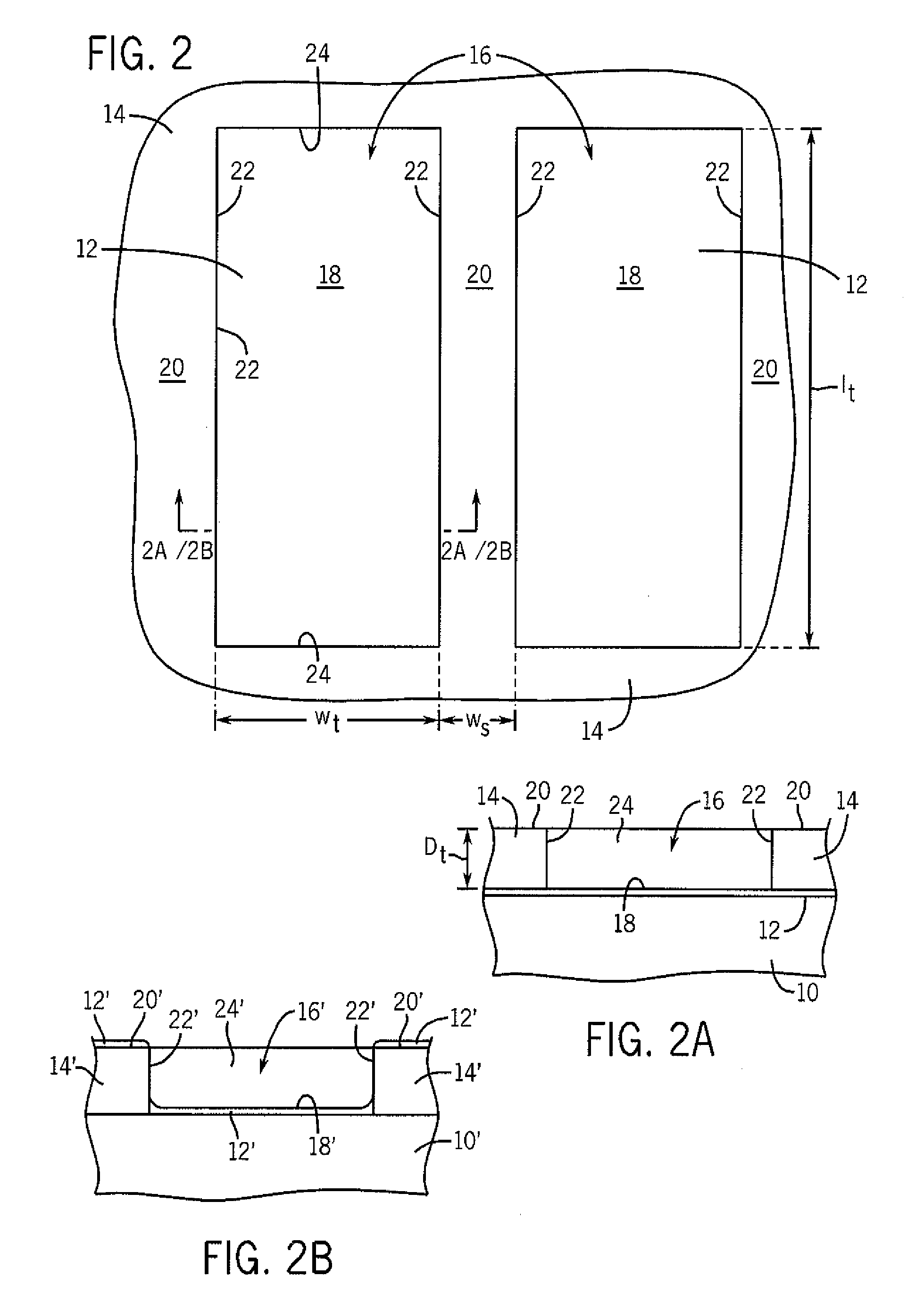
[0023]In the context of the current application, the term “semiconductor substrate” or “semiconductive substrate” or “semiconductive wafer fragment” or “wafer fragment” or “wafer” will be understood to mean any construction comprising semiconductor material, including but not limited to bulk semiconductive materials such as a semiconductor wafer (either alone or in assemblies comprising other materials thereon), and semiconductive material layers (either alone or in assemblies comprising other materials). The term “substrate” refers to any supporting structure including, but not limited to, the semiconductive substrates, wafer fragments or wafers described above.
[0024]“Lo” is the inherent pitch (bulk period or repeat unit) of structur...
PUM
| Property | Measurement | Unit |
|---|---|---|
| Nanoscale particle size | aaaaa | aaaaa |
| Thickness | aaaaa | aaaaa |
| Pressure | aaaaa | aaaaa |
Abstract
Description
Claims
Application Information