Micromechanical device for infrared sensing

a micromechanical and infrared sensing technology, applied in measurement devices, optical radiation measurement, instruments, etc., can solve the problems of increasing the weight, volume, power consumption, and difficulty in limiting the use of infrared imaging devices, and achieve enhanced thermal response time, without adversely affecting the responsivity of the pixel, and enhanced responsivity without adversely affecting the thermal properties of the pixel

Inactive Publication Date: 2009-01-01
FLIR COMML SYST
View PDF11 Cites 18 Cited by
  • Summary
  • Abstract
  • Description
  • Claims
  • Application Information

AI Technical Summary

Benefits of technology

[0022]An object of the present invention is to provide a micromechanical pixel with enhanced responsivity without adversely affecting thermal properties of the pixel.
[0023]Another object of the present invention is to provide a micromechanical pixel with enhanced thermal response time without adversely affecting responsivity of the pixel.
[0024]The present invention is a micromechanical device for infrared sensing with improved thermal sensitivity and thermal response time. Performance of sensing element within the micromechanical device is improved by increasing its absorption efficiency and greater control of light reflected therefrom. Performance of the bending elements within the micromechanical device is improved by increasing their sensitivity to thermal loading and isolating the sensing element and innermost bi-layer cantilever from the outermost bi-layer cantilever and substrate. The design features described below may be implemented alone or combined within a pixel, as described in the Detailed Description of the Invention.

Problems solved by technology

However, the high cost of infrared imaging devices remains a challenge, thereby limiting their use.
However, photon detectors must be cryogenically cooled, thus increasing the weight, volume, and power consumption of presently known devices.
Furthermore, materials which are highly quantum efficiency are notoriously difficult to process and costly.
As such, imaging devices based on photon detector technologies are limited to specialized applications within the fields of national defense and astronomy.
While less costly than photon detector devices, thermal detector devices are affordable within the fields of industrial monitoring and firefighting, yet too costly for most consumer and many industrial applications.
However, the sensitivity of presently known cantilevers is poor because of their low absorption efficiency and large mass.
However, the micromechanical pixel 3 in FIG. 2 suffers from several deficiencies, which limit sensitivity and contribute to sensor noise, including a low fill factor, poor reflector flatness, and mechanical complexity.

Method used


Image

  • Micromechanical device for infrared sensing
  • Micromechanical device for infrared sensing
  • Micromechanical device for infrared sensing

Examples


Embodiment Construction

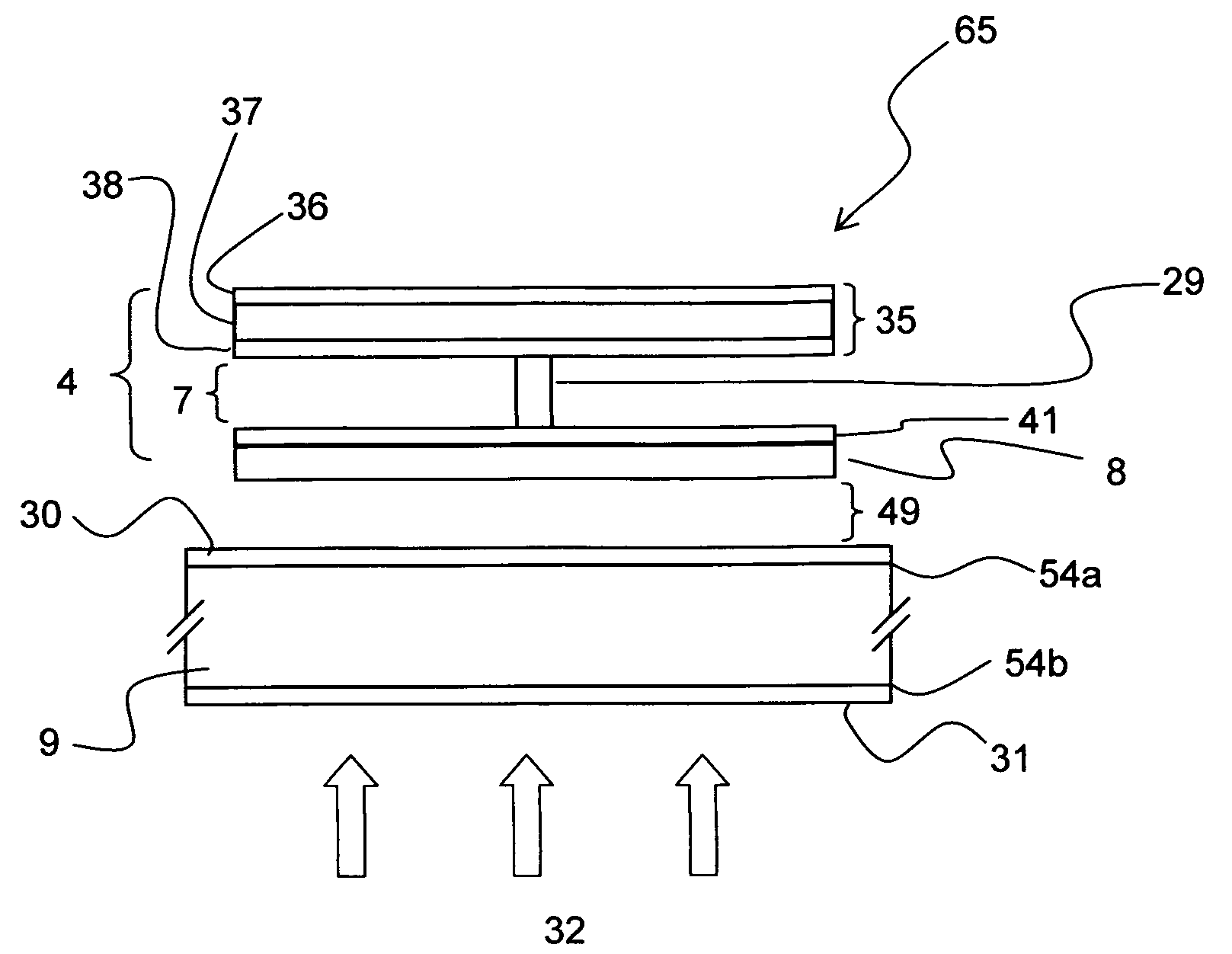
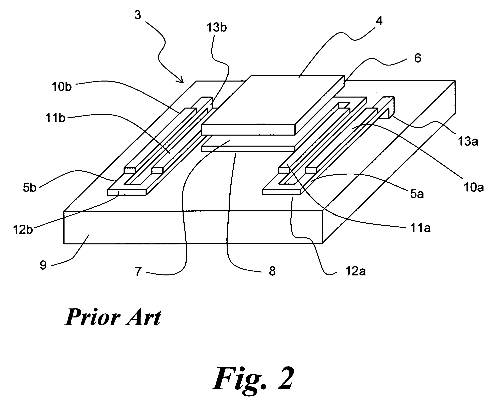
[0058]Embodiments of the present micromechanical device 65 are described with reference to the micromechanical pixel 3 shown in FIG. 2. However, the present invention is applicable within a wide variety of micromechanical pixels that rely on mechanical deflection in response to infrared absorption to generate an optically readable signal.

[0059]Accordingly, the description of and drawing for embodiments for the present invention provided below describe and show design features of the new micromechanical device 65 without further reference to features the embodiment may have with other micromechanical devices. The embodiments described below may be fabricated via micromechanical methods and processes understood in the art.

[0060]Referring now to FIG. 6a, the sensing element 4 of a micromechanical device 65 with backside illumination 32 includes a layered reflector 35, an optical absorption cavity 7, and an absorber layer 8. The layered reflector 35 is constructed to have a multi-layere...


PUM


Abstract

A micromechanical device including an improved sensing element and improved bending elements is described. Sensing elements include multi-layered structures which are thinner, lighter, and flatter than structures presently known within the related arts. Bending elements include structures which separately respond to illumination by an infrared source so as to twist a sensing element. Micromechanical pixels may be arranged to form two-dimensional arrays of infrared sensitive pixels. Arrays of micromechanical pixels are applicable to imaging devices for use within the fields of security and surveillance, firefighting, automotive safety, and industrial monitoring.

Description

CROSS REFERENCE TO RELATED APPLICATIONS[0001]This application is based upon and claims priority under 35 U.S.C. § 119(e) from U.S. Provisional Application No. 60 / 929,518 filed Jun. 29, 2007, entitled High Sensitivity Radiation Detector and Radiation Imaging Device, the contents of which are hereby incorporated in their entirety by reference thereto.FEDERALLY SPONSORED RESEARCH AND DEVELOPMENT[0002]None.BACKGROUND OF THE INVENTION[0003]1. Field of the Invention[0004]The present invention generally relates to a micromechanical device for use within infrared imaging devices. Specifically, the invention is a micromechanical pixel including improved sensing and bending elements which separately and in combination increase the sensitivity and decrease the response time of the pixel.[0005]2. Description of the Related Art[0006]Infrared imaging devices enable a user to view an object via the infrared band of the spectrum, which is otherwise invisible to the human eye. Infrared imaging devic...

Claims


Application Information

Patent Timeline
Patent Type & Authority Applications(United States)
IPC IPC(8): G01J5/02
CPCG01J5/02G01J5/40G01J5/023
Inventor ERDTMANN, MATTHEWZHAO, JINGJIN, GUANGHAI
Owner FLIR COMML SYST
Why Eureka
Try Eureka