
Generation and distribution of a fluorine gas
a technology of fluorine gas and gas storage, which is applied in the direction of plasma technique, non-pressure vessel, solid-state device, etc., can solve the problems of process obviating the need and inherent risks, and gasses may have limited shelf li
- Summary
- Abstract
- Description
- Claims
- Application Information
AI Technical Summary
Problems solved by technology
Method used
Image

Examples
examples
Plasma Etch Example
[0049]An aluminum-containing layer can be formed to a thickness of approximately 800 nm. After subsequent patterning, bond pads having areal dimensions of 15 microns by 15 microns, nominally, may be formed. A passivation layer may be formed over the bond pads and have a thickness of approximately 900 nm. The passivation layer may comprise approximately 200 nm of silicon oxide and approximately 700 nm of silicon nitride. One or both of the silicon oxide and silicon nitride layers may be formed using plasma-enhanced chemical vapor deposition.
[0050]A patterned photoresist layer can be formed over the passivation layer. In one non-limiting embodiment, the photoresist layer may be JSR positive photoresist material available from JSR Company of Japan and has a thickness of approximately 3500 nm. The patterned photoresist comprise opening over the bond pads.
[0051]The passivation layer can be etched with an etchant gas composition comprising diatomic fluorine (F2), carbon...
process example
Plasma Cleaning Process Example
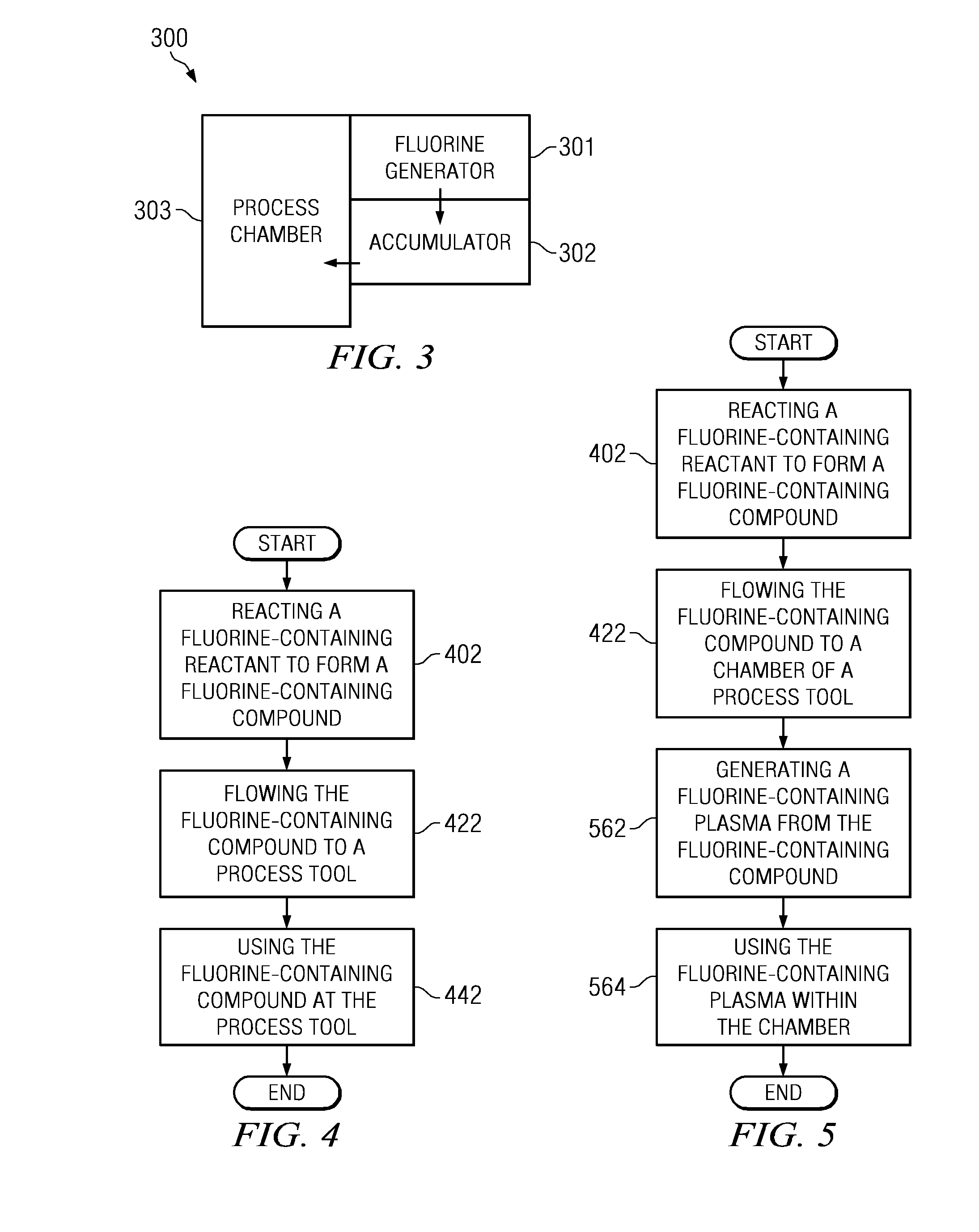
[0053]In a more specific exemplary process, a gas capable of reacting with the deposits to be removed may be flowed into a space to be cleaned, e.g., the vacuum deposition chamber. The deposits may be a silicon-containing material, a metal containing material (e.g., a metal, a metal alloy, a metal silicide, etc.) or the like. The gas can be excited to form a plasma within the chamber or remote to the chamber. If formed outside the chamber, the plasma can flow to the chamber using a conventional downstream plasma process. The plasma or neutral radicals generated from the plasma can react with the deposits on the exposed surfaces within the chamber.
[0054]The gas employed in the etching process typically is a gaseous source of a halogen. The gaseous source may include F2, NF3, SF6, CF4, C2F6 combinations thereof, or the like. Additionally, chlorine-containing or bromine-containing gases may be used. In a non-limiting specific embodiment, F2 may have previ...
PUM
| Property | Measurement | Unit |
|---|---|---|
| Size | aaaaa | aaaaa |
| Distribution | aaaaa | aaaaa |
Abstract
Description
Claims
Application Information