
Led with Phosphor Layer Having Different Thickness or Different Phosphor Concentration

Active Publication Date: 2009-01-01
PANASONIC CORP
View PDF4 Cites 69 Cited by
  • Summary
  • Abstract
  • Description
  • Claims
  • Application Information

AI Technical Summary

Benefits of technology

[0013]A second method for manufacturing a light-emitting device of the present invention is a method for manufacturing a light-emitting device including a substrate, a light-emitting element that is mounted on the substrate and includes a luminous region and a nonluminous region, and a phosphor layer that is formed to cover t

Problems solved by technology

Thus, the luminescent color of the light-emitting device 100 is not uniform, which can make it difficult to use the device in a lighting unit or a display unit.

Method used


Image

  • Led with Phosphor Layer Having Different Thickness or Different Phosphor Concentration
  • Led with Phosphor Layer Having Different Thickness or Different Phosphor Concentration
  • Led with Phosphor Layer Having Different Thickness or Different Phosphor Concentration

Examples


embodiment 1

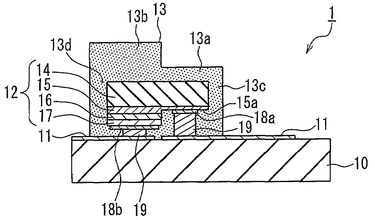
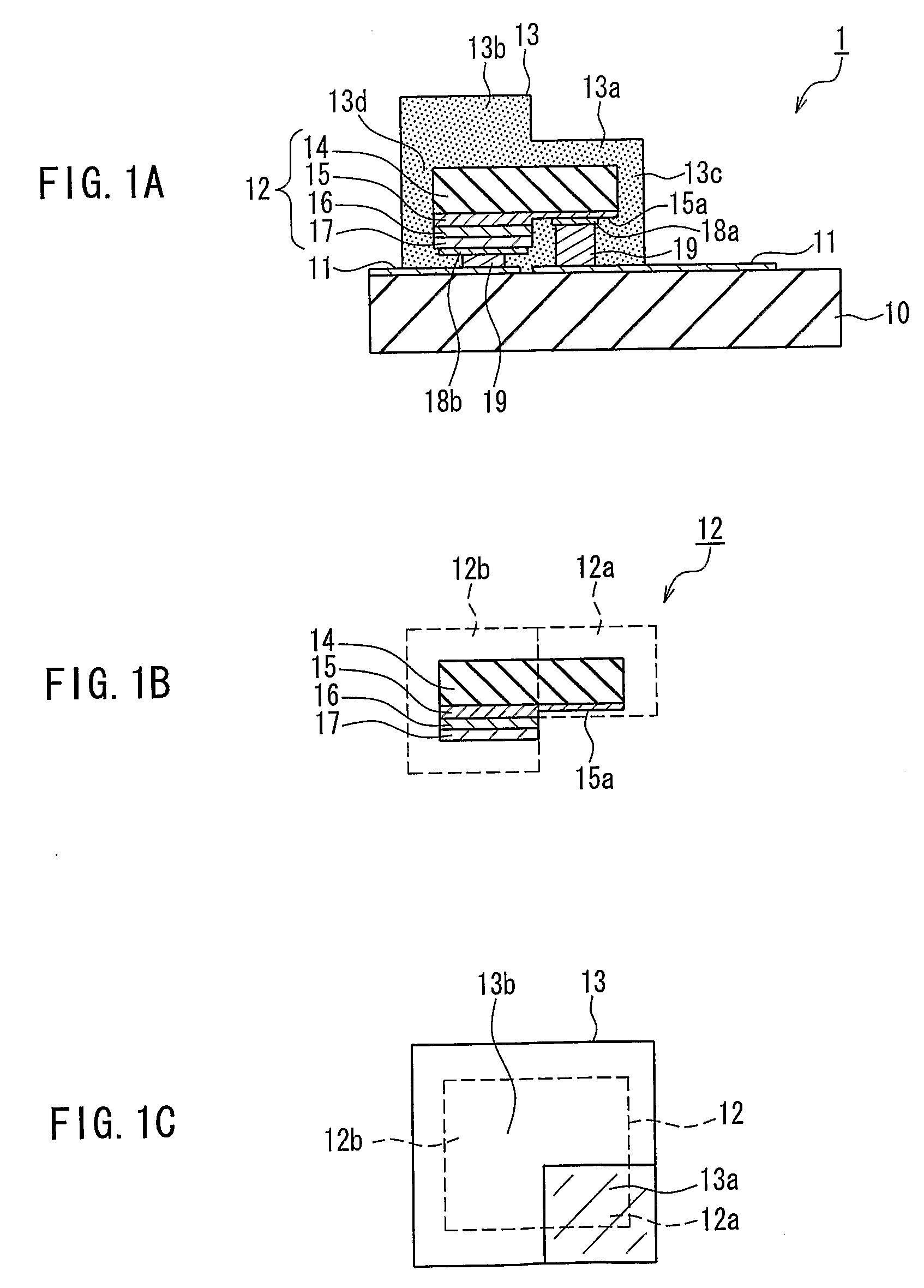
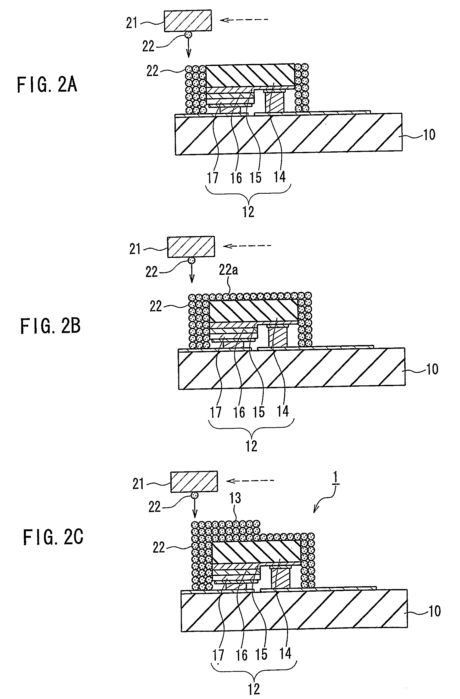
[0046]A light-emitting device of Embodiment 1 of the present invention will be described with reference to the drawings. FIG. 1A is a cross-sectional view showing the light-emitting device of Embodiment 1. FIG. 1B is a cross-sectional view showing an LED chip included in the light-emitting device of FIG. 1A. FIG. 1C is a top view showing a phosphor layer and the LED chip included in the light-emitting device of FIG. 1A. The light-emitting device of Embodiment 1 is an example of the first light-emitting device of the present invention.

[0047]As shown in FIG. 1A, the light-emitting device 1 includes a substrate 10, a conductor pattern 11 that is formed on the substrate 10, an LED chip 12 that is flip-chip mounted on the conductor pattern 11, and a phosphor layer 13 that is formed to cover the LED chip 12 and includes a phosphor.

[0048]The LED chip 12 includes a sapphire substrate 14 and a first conductivity-type layer 15, a light-emitting layer 16, and a second conductivity-type layer 1...

embodiment 2

[0063]A light-emitting device of Embodiment 2 of the present invention will be described with reference to the drawings. FIG. 5A is a cross-sectional view showing the light-emitting device of Embodiment 2. FIG. 5B is a cross-sectional view showing an LED chip included in the light-emitting device of FIG. 5A. FIG. 5C is a top view showing a phosphor layer and the LED chip included in the light-emitting device of FIG. 5A. The light-emitting device of Embodiment 2 is an example of the second light-emitting device of the present invention. In FIGS. 5A to 5C, the same components as those in FIGS. 1A to 1C are denoted by the same reference numerals, and the explanation will not be repeated.

[0064]As shown in FIG. 5A, the light-emitting device 2 of Embodiment 2 differs from the light-emitting device 1 (see FIG. 1A) of Embodiment 1 only in the phosphor layer. In a phosphor layer 20 of the light-emitting device 2, the concentration of the phosphor in a first phosphor layer 20a located on the ...

embodiment 3

[0073]A display unit of Embodiment 3 of the present invention will be described by referring to the drawings. FIG. 8 is a perspective view showing the display unit (image display apparatus) of Embodiment 3.

[0074]As shown in FIG. 8, the image display apparatus 4 of Embodiment 3 includes a panel 40. A plurality of light-emitting modules 3 are arranged in a matrix form on a principal surface 40a of the panel 40 as light sources. The image display apparatus 4 with this configuration uses the light-emitting modules 3, each of which includes the light-emitting device 1 of the present invention, as light sources and thus can suppress nonuniform luminescent color.


PUM


Abstract

A light-emitting device (1) includes a substrate (10), a light-emitting element (12) that is mounted on the substrate (10) and includes a luminous region (12b) and a nonluminous region (12a), and a phosphor layer (13) that is formed to cover the light-emitting element (12). The thickness of the phosphor layer (13a) located on the nonluminous region (12a) is smaller than that of the phosphor layer (13b) located on the luminous region (12b). The light-emitting device (1) can suppress nonuniform luminescent color.

Description

TECHNICAL FIELD[0001]The present invention relates to a light-emitting device that uses a light-emitting element including luminous and nonluminous regions, a display unit and a lighting unit that use the light-emitting device, and a method for manufacturing the light-emitting device.BACKGROUND ART[0002]A light-emitting diode (referred to as “LED” in the following) is known as a light-emitting element including a semiconductor multilayer film. In particular, when a LED for emitting blue light such as a GaN LED is combined with a phosphor that emits yellow light by excitation of the blue light, the LED can be applied to a light-emitting device for emitting white light (e.g., JP 2001-15817 A).[0003]FIGS. 12A and 12B show a conventional light-emitting device. FIG. 12A is a schematic top view of the light-emitting device, and FIG. 12B is a cross-sectional view taken along the line I-I in FIG. 12A.[0004]As shown in FIGS. 12A and 12B, a light-emitting device 100 includes a substrate 101, ...

Claims


Application Information

Patent Timeline
IPC IPC(8): H01J1/62H01J9/00H01L33/32H01L33/50
CPCH01L33/507H01L33/508H01L2933/0041H01L2224/13H01L2224/48091H01L2224/45144H01L2924/00014H01L2924/00H01J1/62H01L2224/0554H01L2224/05568H01L2224/05573H01L2224/05599H01L2224/0555H01L2224/0556
Inventor TANIMOTO, NORIYASUOGATA, TOSHIFUMISHIDA, SATOSHINAITO, HIROYUKI
Owner PANASONIC CORP
Features
  • Generate Ideas
  • Intellectual Property
  • Life Sciences
  • Materials
  • Tech Scout
  • Unparalleled Data Quality
  • Higher Quality Content
  • 60% Fewer Hallucinations
Learn More