Light-emitting device, method for manufacturing the same, and electronic apparatus

a technology of light-emitting devices and electronic devices, which is applied in the direction of discharge tubes/lamp details, organic semiconductor devices, discharge tubes/lamp details, etc., can solve the problems of reducing the reliability of light-emitting elements, short circuit between electrodes, and the reduction of the light-emitting region of pixels, so as to achieve fewer defects, increase the thickness of films, and improve reliability

Inactive Publication Date: 2009-01-01
SEMICON ENERGY LAB CO LTD
View PDF17 Cites 19 Cited by
  • Summary
  • Abstract
  • Description
  • Claims
  • Application Information

AI Technical Summary

Benefits of technology

[0024]In the present invention, the buffer layer and the partition wall have the same film thickness or almost the same film thickness, and this film thickness can be increased; accordingly, a light-emitting device with higher reliability and fewer defects can be provided.
[0025]Since patterning of a partition wall by photolithography is not required in the present invention, the number of mask steps in the fabrication of the substrate is reduced; therefore, a light-emitting device can be provided at low cost.
[0026]For a material of a partition wall, an organic material is typically used. At the same time, a partition wall of an organic materi

Problems solved by technology

However, if the inclination angle of this partition wall is large, the film thickness of an organic film in a pixel is uneven and peeling occurs between films, which results in a problem called a shrink that is a reduction in light-emitting region of a pixel.
A reduction in a light-emitting region greatly decreases the reliability of a light-emitting element.
Further, other causes of short circuit between electrodes include fine particles or the like which remain over the electrode.
Because a distance between elec

Method used


Image

  • Light-emitting device, method for manufacturing the same, and electronic apparatus
  • Light-emitting device, method for manufacturing the same, and electronic apparatus
  • Light-emitting device, method for manufacturing the same, and electronic apparatus

Examples


embodiment mode 1

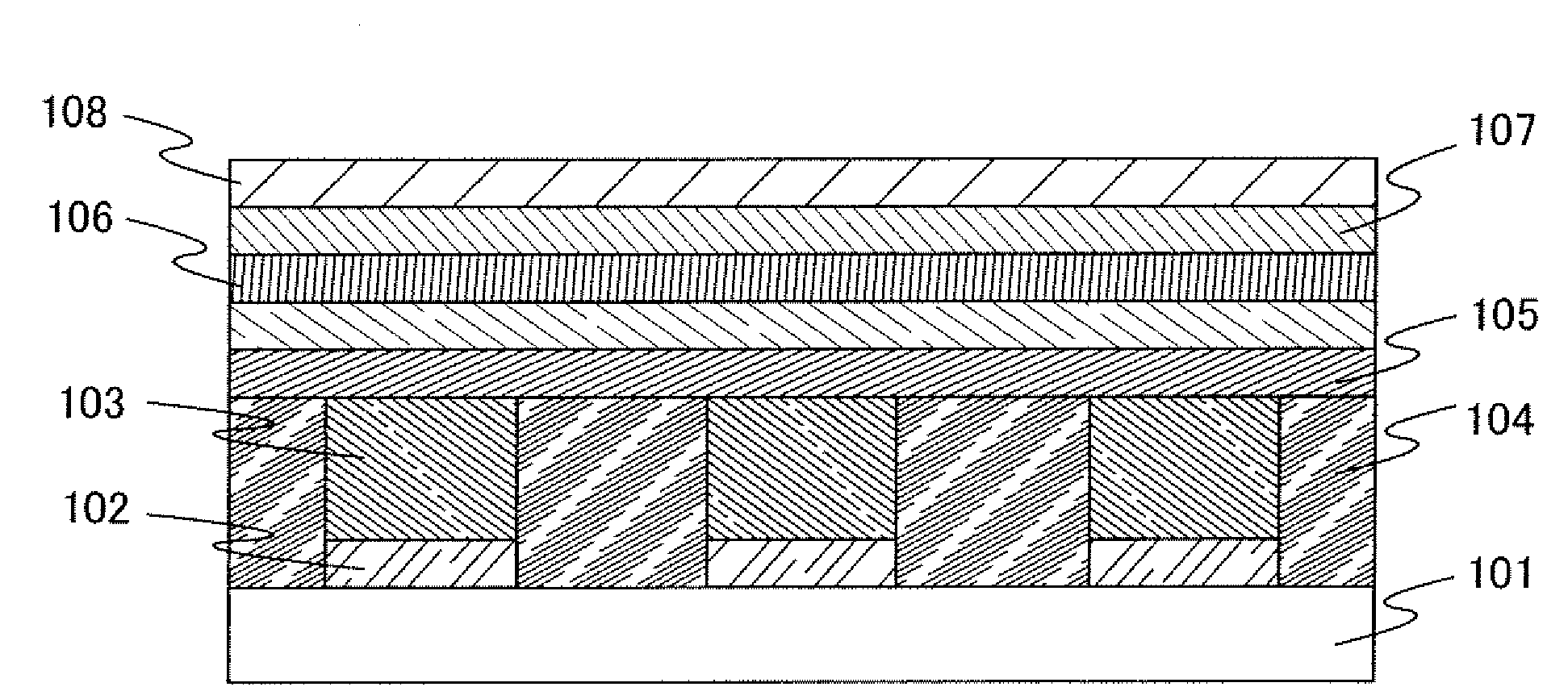
[0037]In this embodiment mode, a light-emitting device of the present invention and a method for manufacturing the light-emitting device are described using FIG. 1.

[0038]The light-emitting device has a light-emitting element in which a plurality of layers is stacked between a pair of electrodes. The plurality of layers is formed by combining and stacking a layer formed of a substance with a high carrier-injecting property and a layer formed of a substance with a high carrier-transporting property so that a light-emitting region is formed apart from the electrodes, in other words, carriers are recombined in a portion apart from the electrodes. In the light-emitting device of the present invention, a plurality of light-emitting elements is provided, and a partition wall 104 is provided between the light-emitting elements.

[0039]In this embodiment mode, the light-emitting element includes a first electrode 102, a second electrode 108, a buffer layer 103, a hole-transporting layer 105, a...

embodiment mode 2

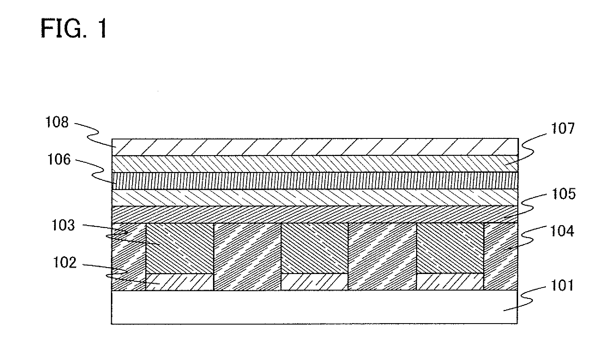
[0068]In this embodiment mode, a method for forming a buffer layer 204 and a partition wall 205 as described in Embodiment Mode 1 is described. As described in Embodiment Mode 1, the buffer layer 204 and the partition wall 205 have the same film thickness or almost the same film thickness. In addition, the buffer layer and the partition wall contains the same kind of organic compound and the same kind of inorganic compound, and the buffer layer 204 further contains a simple substance of a halogen.

[0069]In FIGS. 2A and 2B, several divided first electrodes 202 are provided over a substrate 201. FIG. 2A is a cross-sectional view, and FIG. 2B is a top view. The first electrode 202 corresponds to each pixel and is disposed in a pixel region 301. In the sealing region 302, a sealing material is disposed so as to surround the pixel region. Desirably, no organic material exists under the sealing material. In addition, desirably, no organic material exists in a contact portion 303 of the sec...

embodiment mode 3

[0077]In this embodiment mode, a light-emitting device of the present invention is described.

[0078]In this embodiment mode, the light-emitting device of the present invention is described using FIGS. 5A and 5B. FIG. 5A is a top view of the light-emitting device, and FIG. 5B is a cross-sectional view taken along lines A-A′ and B-B′ of FIG. 5A. The light-emitting device has a driver circuit portion (a source side driver circuit) 601, a pixel portion 602, and a driver circuit portion (a gate side driver circuit) 603 to control the light-emitting device, which are indicated by dotted lines. Reference numerals 604 and 605 denote a sealing substrate and a sealing material, respectively. A portion enclosed by the sealing material 605 corresponds to a space 607.

[0079]A lead wiring 608 is used to transmit signals to be inputted to the source side driver circuit 601 and the gate side driver circuit 603 and receives a video signal, a clock signal, a start signal, a reset signal, and the like f...


PUM

PropertyMeasurementUnit
Fractionaaaaaaaaaa
Fractionaaaaaaaaaa
Thicknessaaaaaaaaaa

Abstract

The present invention provides a light-emitting device including a light-emitting element over a substrate, the light-emitting element is partitioned from an adjacent light-emitting element by a partition wall, the light-emitting element comprising a first electrode, a layer formed over the first electrode, a light-emitting layer formed over the layer and a second electrode formed over the light-emitting layer, the layer contains an inorganic compound, an organic compound and a halogen atom, the partition wall contains the inorganic compound and the organic compound, and the layer. The light-emitting device provides higher reliability and fewer defects.

Description

BACKGROUND OF THE INVENTION[0001]1. Field of the Invention[0002]The present invention relates to a light-emitting device, a method for manufacturing the same, and an electronic apparatus.[0003]2. Description of the Related Art[0004]In recent years, research and development have been actively conducted on light-emitting elements using electroluminescence. In a basic structure of such a light-emitting element, a layer containing a substance with a light-emitting property is interposed between a pair of electrodes. By application of a voltage to this element, light emission can be obtained from a substance with a light-emitting property.[0005]This kind of light-emitting element, which is a self-luminous element, is advantageous in that pixel visibility is high compared to that of a liquid crystal display, that no backlight is needed, and the like and thought to be suitable for use as a flat panel display element. In addition, this kind of light-emitting element is highly advantageous i...

Claims


Application Information

Patent Timeline
IPC IPC(8): H01L51/40H01J1/63
CPCH01L51/5052H01L51/5088H01L2251/558H01L51/52H01L51/5215H01L27/3283H01L2251/5392H01L51/002H10K59/173H10K71/30H10K50/155H10K50/165H10K50/17H10K50/816H10K2102/341H10K2102/351H10K50/80
Inventor IKEDA, HISAOIBE, TAKAHIROKOEZUKA, JUNICHIKATO, KAORU
Owner SEMICON ENERGY LAB CO LTD
Why Eureka
Try Eureka