

Display device
a display device and display layer technology, applied in non-linear optics, instruments, optics, etc., can solve the problem of high reliability that cannot be obtained in the display device, and achieve the effect of preventing the deterioration of the display layer, high reliability, and high efficiency in the use of materials
- Summary
- Abstract
- Description
- Claims
- Application Information
AI Technical Summary
Benefits of technology
Problems solved by technology
Method used
Image

Examples
embodiment mode 1
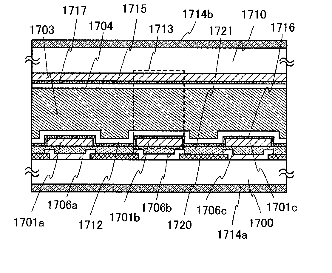
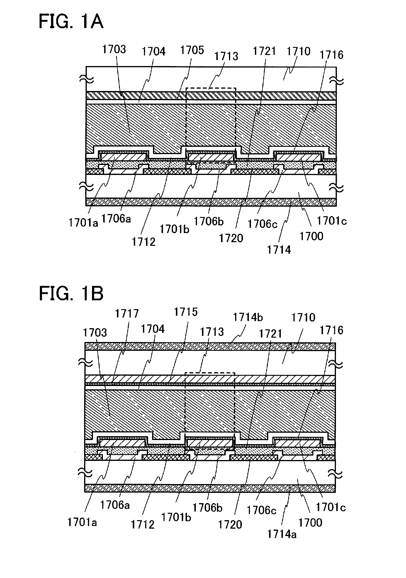
[0054]This embodiment mode will describe an example of a display device aimed at higher image quality and higher reliability, which can be manufactured at low cost with high productivity. Specifically, this embodiment mode will describe a display device having a passive-matrix structure.
[0055]FIGS. 1A and 1B each show a passive matrix liquid crystal display device to which the present invention is applied. FIG. 1A shows a reflective liquid crystal display device and FIG. 1B shows a transmissive liquid crystal display device. In FIGS. 1A and 1B, a substrate 1700 and a substrate 1710 face each other with a liquid crystal layer 1703 sandwiched therebetween. In FIG. 1A, electrode layers 1701a, 1701b, and 1701c also referred to as pixel electrode layers, which are used for display elements 1713, an inorganic insulating film 1716, an insulating layer 1712 serving as an alignment film, color layers 1706a, 1706b, and 1706c serving as color filters, a light blocking layer 1720, an insulating...
embodiment mode 2
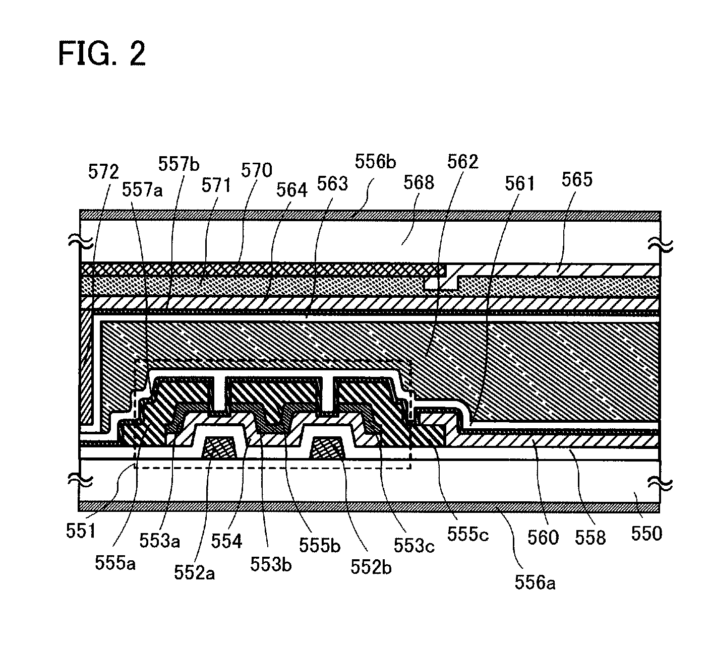
[0102]This embodiment mode will describe an example of a display device aimed at higher image quality and higher reliability, which can be manufactured at low cost with high productivity. In this embodiment mode, a display device having a different structure from the above-described display device in Embodiment Mode 1 is described. Specifically, this embodiment mode will describe a display device having an active-matrix structure.
[0103]FIG. 2 shows an active matrix liquid crystal display device to which the present invention is applied. In FIG. 2, a substrate 550 provided with a transistor 551 having a multi-gate structure, an electrode layer 560 of a display element, an inorganic insulating film 557a, an insulating layer 561 serving as an alignment film, and a polarizer (also referred to as a polarizing plate) 556a; and a substrate 568 provided with an insulating layer 563 serving as an alignment film, an electrode layer 564 of a display element, an inorganic insulating film 557b, ...
embodiment mode 3
[0140]This embodiment mode will describe an example of a display device aimed at higher image quality and higher reliability, which can be manufactured at low cost with high productivity. In specific, this embodiment mode describes a liquid crystal display device using a liquid crystal display element as a display element.
[0141]FIG. 4A is a top view of a liquid crystal display device which is one mode of the present invention. FIG. 4B is a cross-sectional view taken along line C-D in FIG. 4A.
[0142]As shown in FIG. 4A, a pixel region 606 and driver circuit regions 608a and 608b which are scan line driver circuits are sealed between a substrate 600 and a counter substrate 695 with a sealant 692. In addition, a driver circuit region 607 which is a signal line driver circuit including a driver IC is provided over the substrate 600. A transistor 622 and a capacitor 623 are provided in the pixel region 606, and a driver circuit including a transistor 620 and a transistor 621 is provided i...
PUM
| Property | Measurement | Unit |
|---|---|---|
| thickness | aaaaa | aaaaa |
| thickness | aaaaa | aaaaa |
| ionization energy | aaaaa | aaaaa |
Abstract
Description
Claims
Application Information