Method for Fabricating Semiconductor Chip

Active Publication Date: 2009-01-01
PANASONIC CORP
View PDF8 Cites 21 Cited by
  • Summary
  • Abstract
  • Description
  • Claims
  • Application Information

AI Technical Summary

Benefits of technology

[0020]The die attach film used as a mask in plasma etching is used, as it is, as an adhesive for a leadframe, a substrate, and the like, after removal of the heat-resistant film. Accordingly, a step of removal (ashing) of a resist film, whic

Problems solved by technology

Incidentally, when a die attach film is exposed to a high-temperature environment which is at a temperature of 100° C. or higher, curing reaction usually proceeds, whereupon the film does not exhibit sufficient function as a bonding agent.
For this reason, affixing of a semiconductor wafer before performance of plasma dicing as described in Patent Document 2 is unrealistic.
However, accurately shaping the small piece of the die attach film affixed to

Method used


Image

  • Method for Fabricating Semiconductor Chip
  • Method for Fabricating Semiconductor Chip
  • Method for Fabricating Semiconductor Chip

Examples


Embodiment Construction

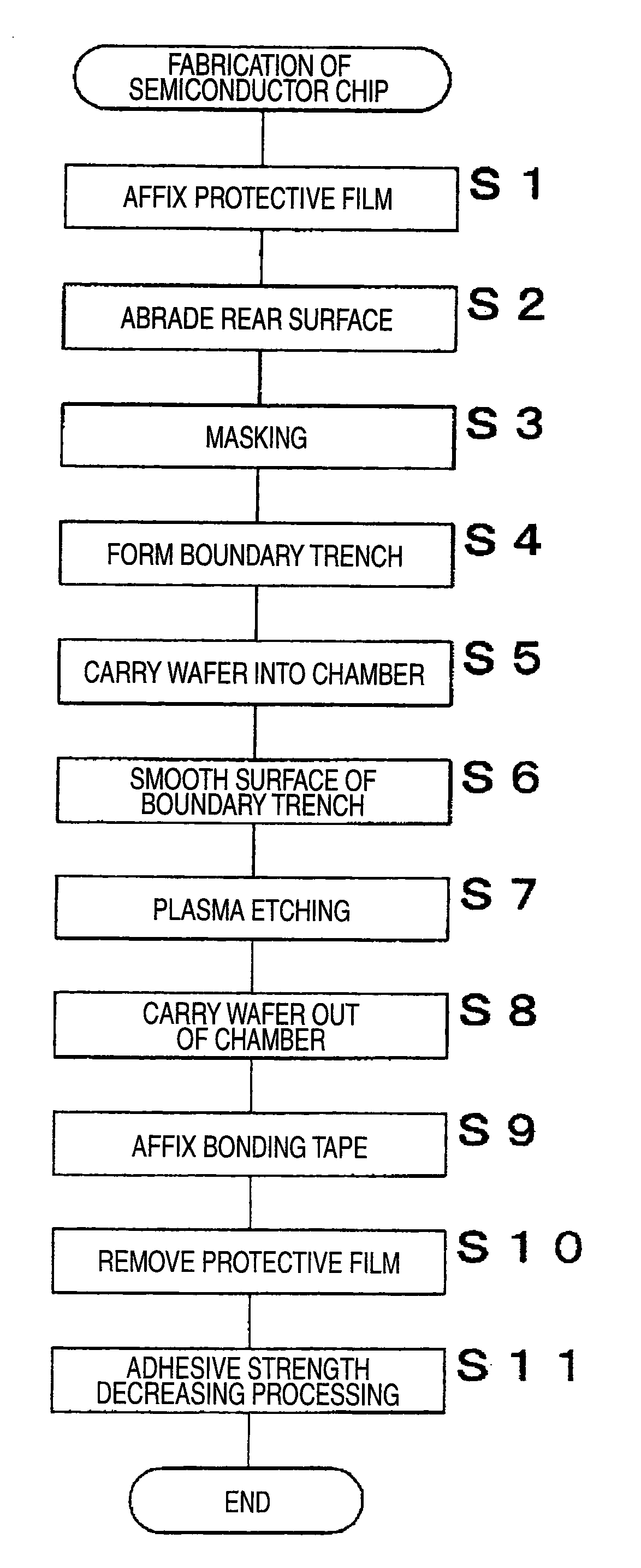
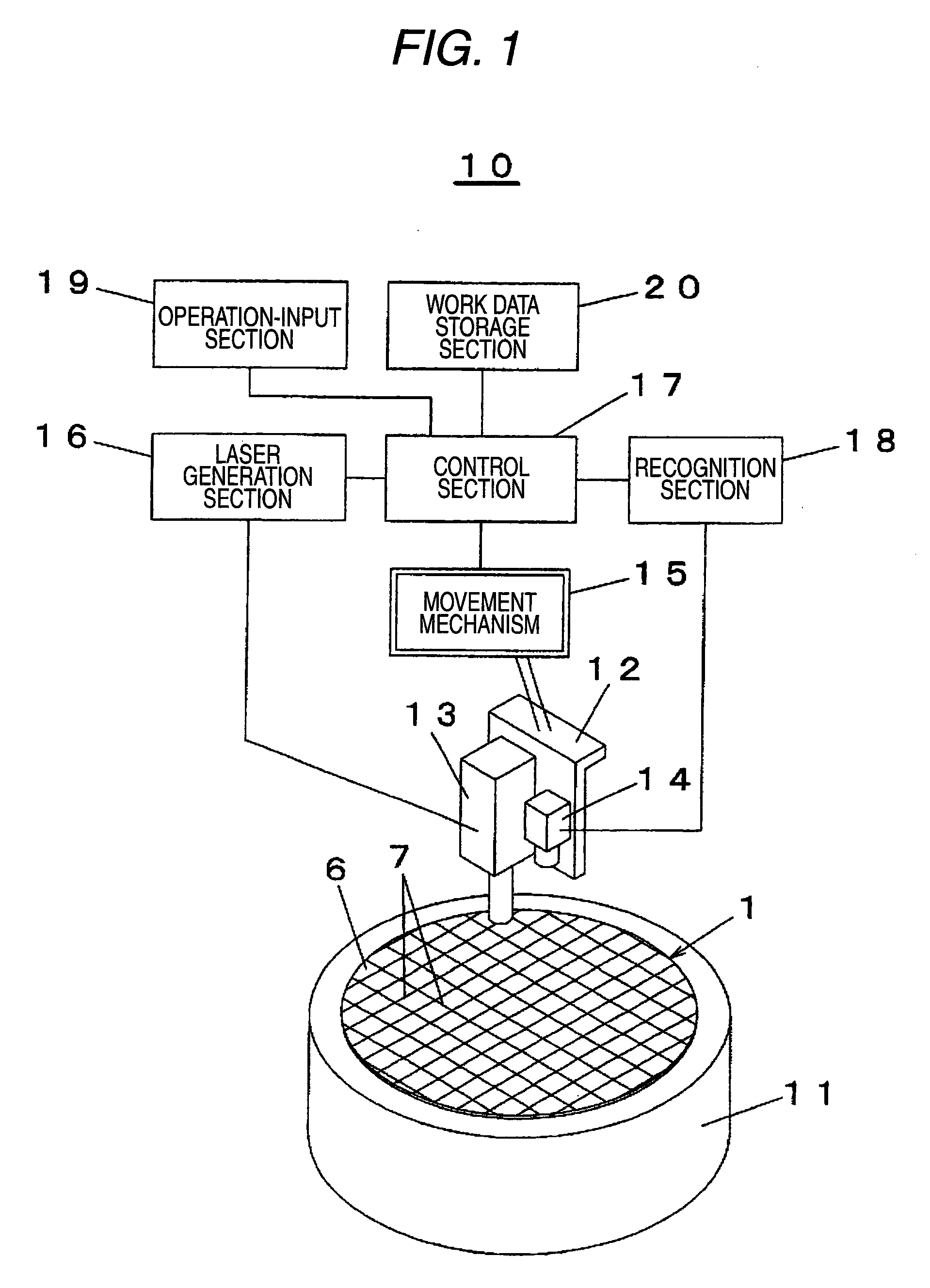
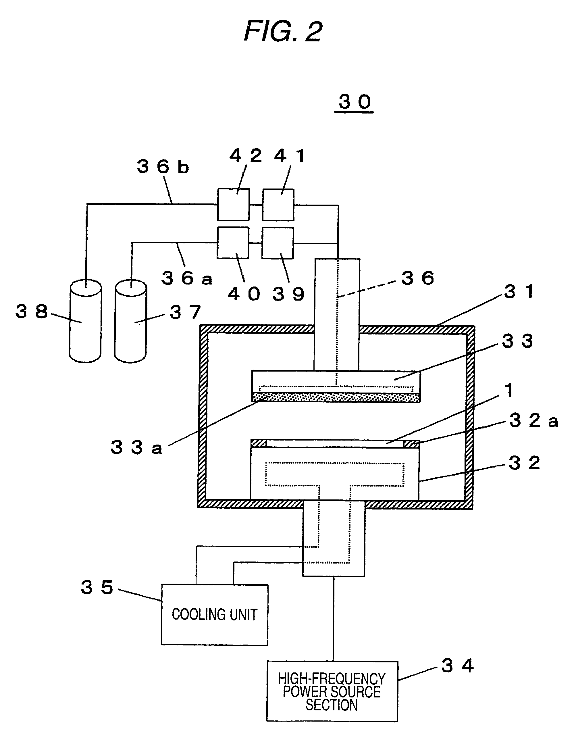
[0029]An embodiment of the present invention will be described hereunder by reference to the drawings. The configuration of a laser beam machining apparatus 10 and a plasma processing apparatus 30 used in implementation of the method for fabricating a semiconductor chip of an embodiment of the present invention will first be described by reference to FIGS. 1 and 2.

[0030]In FIG. 1, the laser beam machining apparatus 10 includes a wafer holding section 11 for holding in a level position a semiconductor wafer 1 which is an object of processing; a moving plate 12 provided in a movable manner at an elevated position above the wafer holding section 11; a laser emission section 13 and a camera 14 which are fixed to the moving plate 12; a movement mechanism 15 for moving the moving plate 12; a laser generation section 16 for causing the laser emission section 13 to generate a laser beam; a control section 17 for controlling driving of the movement mechanism 15 and generation of a laser beam...


PUM

PropertyMeasurementUnit
Electrical resistanceaaaaaaaaaa
Adhesion strengthaaaaaaaaaa

Abstract

After a film layer 6 formed from a die attach film 4 and a UV tape 5 has been provided as a mask on a semiconductor wafer 1, boundary trenches 7 for partitioning semiconductor elements 2 formed on a circuit pattern formation surface 1a are formed in the film layer 6, thereby making a surface 1c of a semiconductor wafer 1 exposed. The exposed surface 1c of the semiconductor wafer 1 in the boundary trenches 7 is etched by means of plasma of a fluorine-based gas, and the semiconductor wafer 1 is sliced into semiconductor chips 1′ along the boundary trenches 7.

Description

TECHNICAL FIELD[0001]The present invention relates to a semiconductor chip fabrication method for fabricating semiconductor chips by slicing a semiconductor wafer through use of plasma dicing.BACKGROUND ART[0002]A related-art process for fabricating a semiconductor includes forming a plurality of semiconductor elements on a circuit pattern formation surface of a semiconductor wafer and subsequently slicing (cutting) the semiconductor wafer, in a mechanical manner, so as to separate the semiconductor elements from each other. A fabricated semiconductor chip is bonded to a leadframe, a substrate, and the like, by means of an epoxy-resin-based liquid adhesive. However, a film-shaped adhesive called a die attach film (DAF) which is easy to handle in connection with a thin semiconductor chip has recently been used.[0003]The die attach film is affixed to a rear surface of a semiconductor wafer (i.e., a surface opposite to a circuit pattern formation surface) before mechanical dicing of th...

Claims


Application Information

Patent Timeline
IPC IPC(8): H01L21/00
CPCB23K26/4065H01L21/78H01L24/743H01L2224/743H01L2924/00B23K2103/42B23K2103/50H01L2924/12042H01L21/3065
Inventor ARITA, KIYOSHIHAJI, HIROSHI
Owner PANASONIC CORP
Why Eureka
Try Eureka