Method for forming a dual metal gate structure

Active Publication Date: 2009-01-01
NXP USA INC
View PDF11 Cites 3 Cited by
  • Summary
  • Abstract
  • Description
  • Claims
  • Application Information

AI Technical Summary

Problems solved by technology

In the field of semiconductor processing, the use of polysilicon gate structures is becoming increasingly less feasible as gate dielectric thicknesses steadily decrease.
As semiconductor processing moves away from the use of silicon dioxide as gate dielectrics in favor of dielectrics having a high dielectric constant (also referred to as high k dielectrics), polysilicon gates become more problematic.
However, in conventional dual metal gate integrations, some processing steps, such as the metal etches and hard mask removals, can damage the high k gate dielectrics of the dual metal gate structures, thus degrading device performance.

Method used


Image

  • Method for forming a dual metal gate structure
  • Method for forming a dual metal gate structure
  • Method for forming a dual metal gate structure

Examples


Embodiment Construction

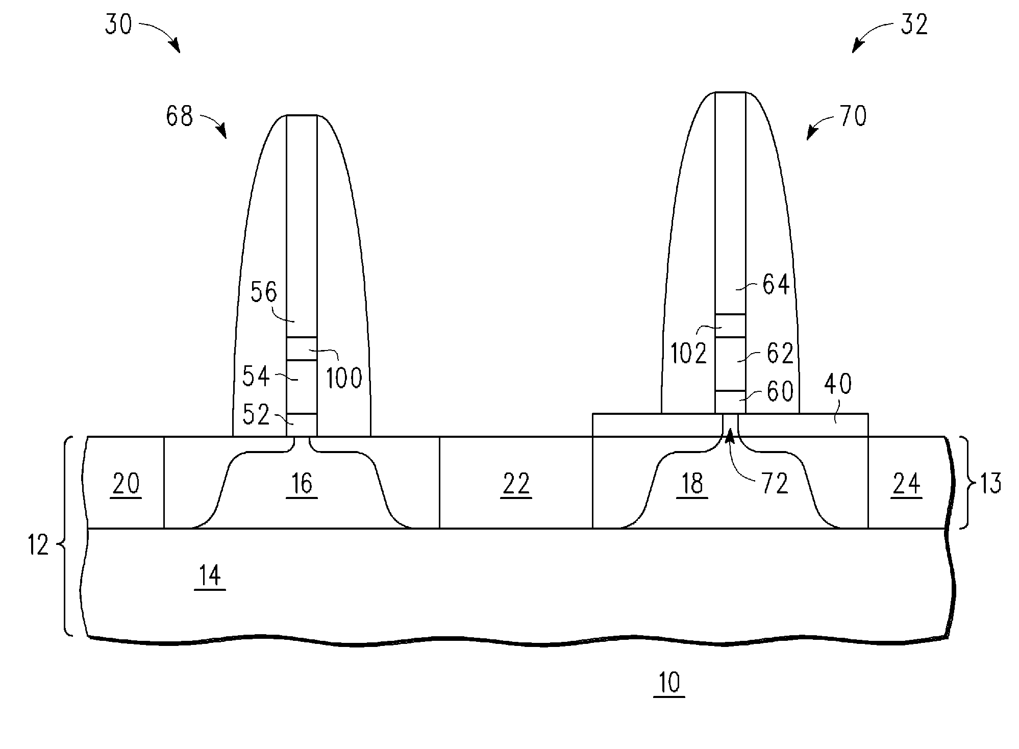
[0020]Dual metal gate integrations where a first metal gate is used for NMOS devices and a second different metal gate is used for PMOS devices may be used to address the problems associated with polysilicon gates and allows for the work functions to be optimized for each type of device. Also, performance of PMOS and NMOS devices can be further improved through the use of different materials for the channel regions of the devices. For example, an NMOS device may perform well when its channel region is formed in one semiconductor material (such as silicon) while a PMOS device may perform better when its channel region is formed in a different semiconductor material (such as silicon germanium). Therefore, one embodiment described below includes a dual metal integration which also allows for different types of channel regions for NMOS and PMOS devices.

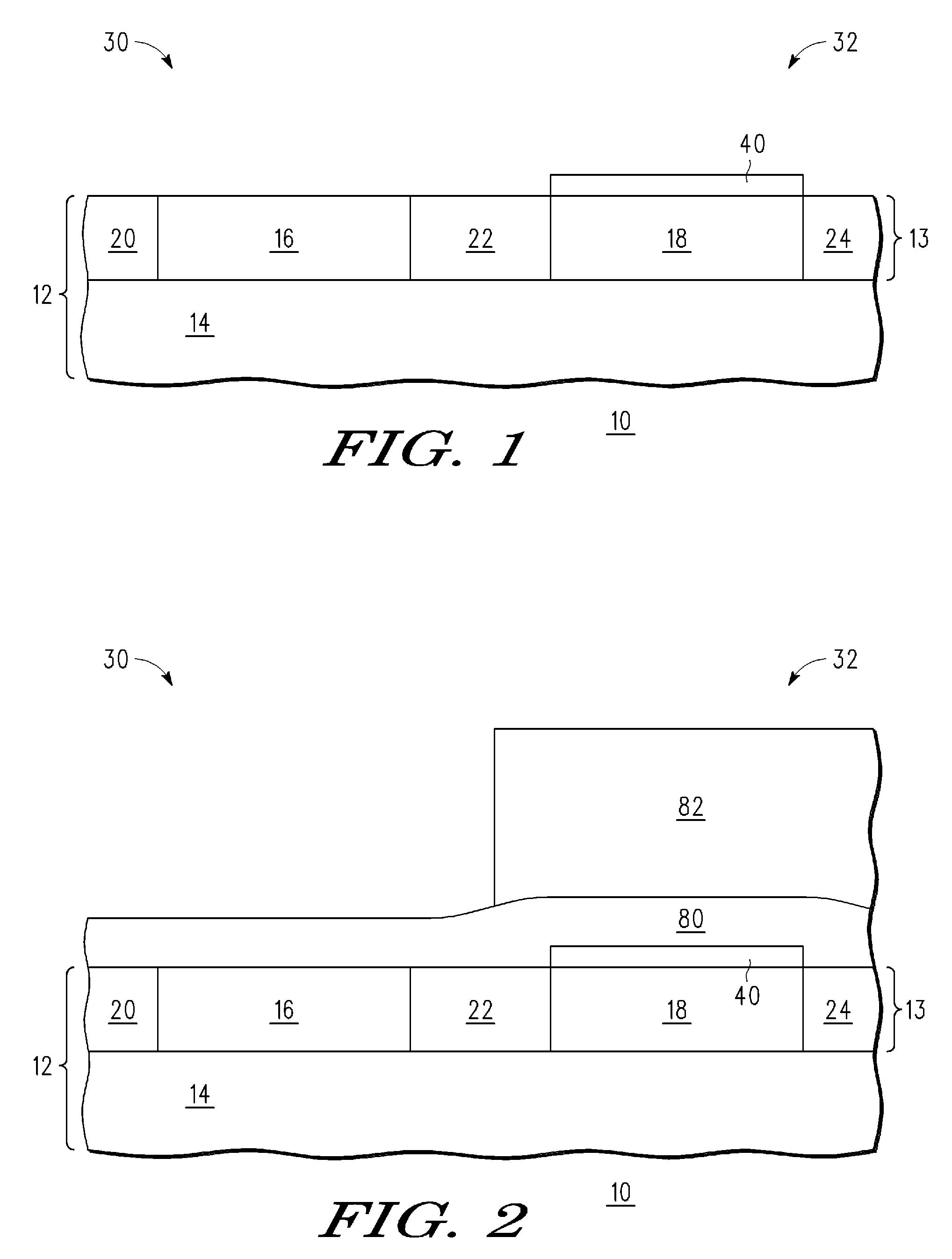
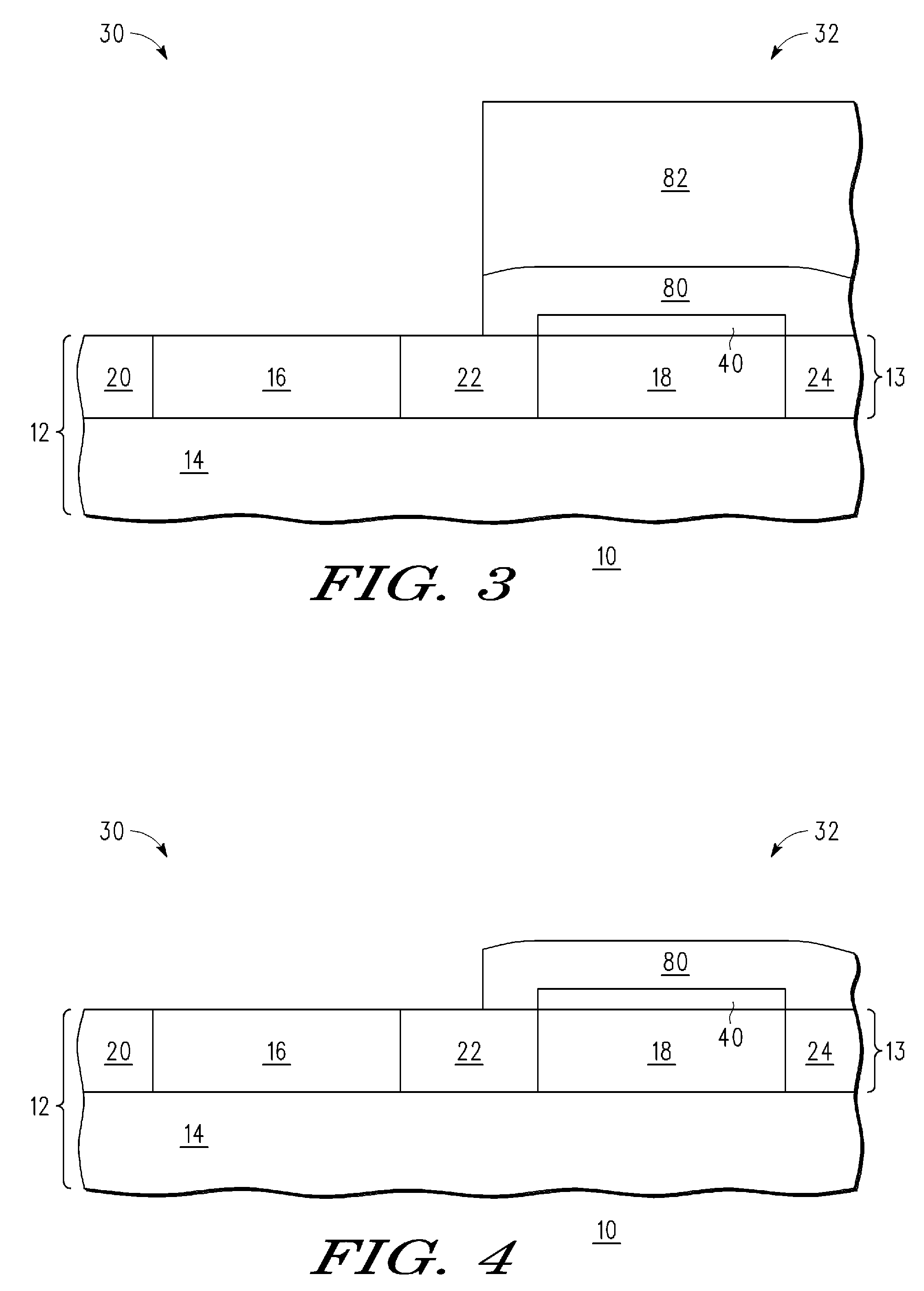
[0021]FIG. 1 illustrates a semiconductor structure 10 having a semiconductor substrate 12. Semiconductor substrate 12 includes a buried ...


PUM


Abstract

A method for forming a semiconductor structure includes forming a channel region layer over a semiconductor layer where the semiconductor layer includes a first and a second well region, forming a protection layer over the channel region layer, forming a first gate dielectric layer over the first well region, forming a first metal gate electrode layer over the first gate dielectric, removing the protection layer, forming a second gate dielectric layer over the channel region layer, forming a second metal gate electrode layer over the second gate dielectric layer, and forming a first gate stack including a portion of each of the first gate dielectric layer and the first metal gate electrode layer over the first well region and forming a second gate stack including a portion of each of the second gate dielectric layer and the second metal gate electrode layer over the channel region layer.

Description

CROSS-REFERENCE TO RELATED APPLICATION(S)[0001]This application is related to U.S. patent spplication Serial No. ______ (Attorney Docket No. MT 10687TP), filed on even date, entitled “Method for Forming a Dual Metal Gate Structure,” naming Gauri V. Karve, Cristiano Capasso, Srikanth B. Samavedam, James K. Schaeffer, and William J. Taylor, Jr., as inventors, and assigned to the current assignee hereof.BACKGROUND[0002]1. Field[0003]This disclosure relates generally to semiconductor processing, and more specifically, to a method for forming a dual metal gate structure.[0004]2. Related Art[0005]In the field of semiconductor processing, the use of polysilicon gate structures is becoming increasingly less feasible as gate dielectric thicknesses steadily decrease. As semiconductor processing moves away from the use of silicon dioxide as gate dielectrics in favor of dielectrics having a high dielectric constant (also referred to as high k dielectrics), polysilicon gates become more problema...

Claims


Application Information

Patent Timeline
IPC IPC(8): H01L21/8238
CPCH01L21/823807H01L21/823857H01L21/823842H01L21/823814
Inventor KARVE, GAURI V.CAPASSO, CRISTIANOSAMAVEDAM, SRIKANTH B.SCHAEFFER, JAMES K.TAYLOR, JR., WILLIAM J.
Owner NXP USA INC
Why Eureka
Try Eureka