Method for memory address arrangement

a memory address and address technology, applied in the field of address arrangement, can solve the problems of increasing access frequency, burden and limitation on hardware configuration, and limiting the configuration of other hardware and software of the system, so as to prevent the limitation of only longitudinal or lateral writing.

Inactive Publication Date: 2009-01-01
NOVATEK MICROELECTRONICS CORP
View PDF6 Cites 4 Cited by
  • Summary
  • Abstract
  • Description
  • Claims
  • Application Information

AI Technical Summary

Benefits of technology

[0008]Accordingly, the present invention is directed to provide a method for memory address arrangement, which is capable of realizing a manner of simultaneously wr

Problems solved by technology

Therefore, the operating frequency of the memory with large capacity is usually too high to be lowered, such that the minimum value of the operating frequency of the system is limited, which brings higher limitations or requirements to the configuration of other hardware and software of the system.
Therefore, it becomes an important technical issue how to lower the access frequency of the memory while keeping or even improving the access speed.
For the longitudinal dividing, it is feasible on theory, but practically, burden and limitation on the hardware configuration c

Method used


Image

  • Method for memory address arrangement
  • Method for memory address arrangement
  • Method for memory address arrangement

Examples


first embodiment

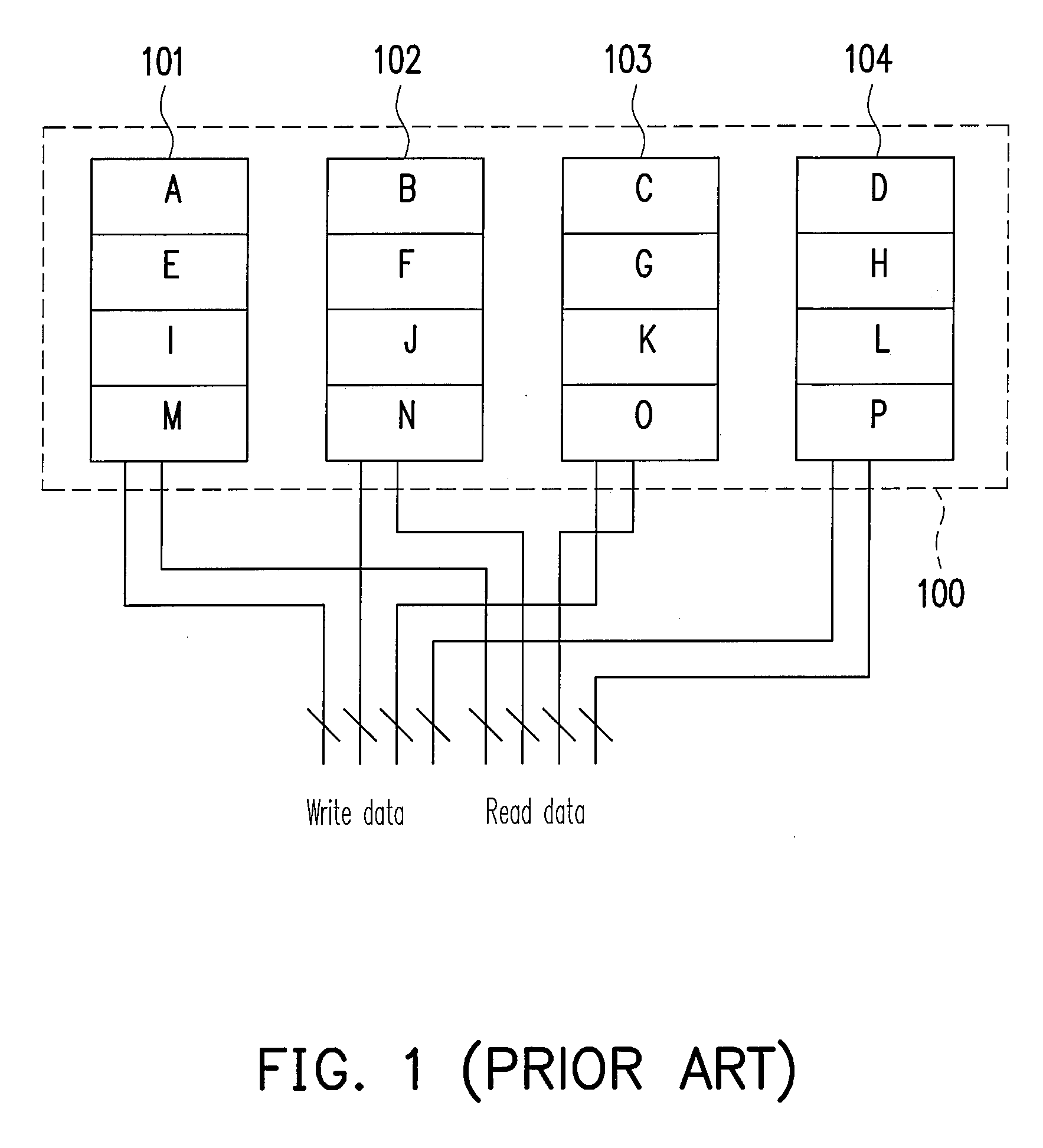
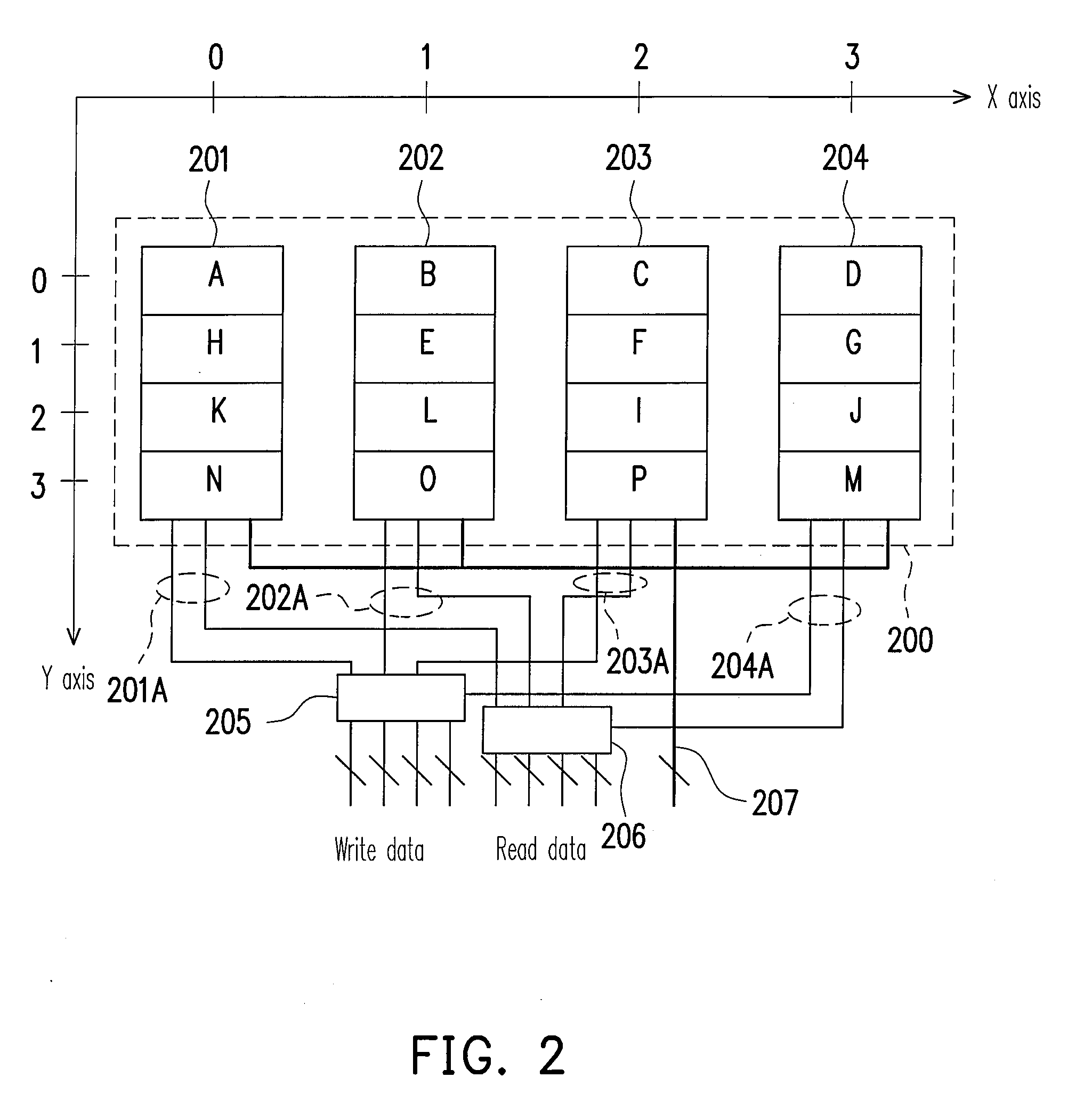
[0030]Next, detailed description is given with examples. In the first embodiment, it is required to continuously read and write four batches of memory data laterally or longitudinally. In FIG. 2 of this embodiment, a related schematic view of the memory in FIG. 1 after the address converting mechanism is added is shown. A memory 200 is laterally divided into sub blocks 201-204, data addresses A-P are address units after the internal moving of the memory, and data lines 201A-204A are respectively address data lines for reading and writing the sub blocks. The main function of a data converter 205 is to convert the data to be written from the external physical position to the corresponding position after the internal moving of the memory. A data converter 206 converts the data to be read from the corresponding address after the internal moving to the external physical position during reading. This can be realized by a multi-to-multi multiplexer. The function of a control signal 207 is ...

second embodiment

[0037]Next, for the second embodiment, it is required to continuously read and write four batches of data laterally or longitudinally to a memory connected to a display panel. FIG. 3 shows the display panel 300, and data addresses A-Z and 1-6 represent the addresses of pixels in the display panel 300. FIG. 4 shows a related schematic view of a memory 400 corresponding to the display panel of FIG. 3 after the address conversion. Sub blocks 401-404 are four laterally divided sub blocks, data converters 405-408 are further provided, a signal 409 is of a value of Y[2], and a read and write data signal 410 is data in the read and write address. Read and write address signals 405B, 406B, 407B, and 408B of the external entity, and a longitudinal read and write signal 411 are input ends of the data converters. The output ends are Y axis shift values represented by signals 405A, 406A, 407A, and 408A, i.e., the value of Y[0:1]. Data addresses A-Z and 1-6 are addresses after the internal movin...

third embodiment

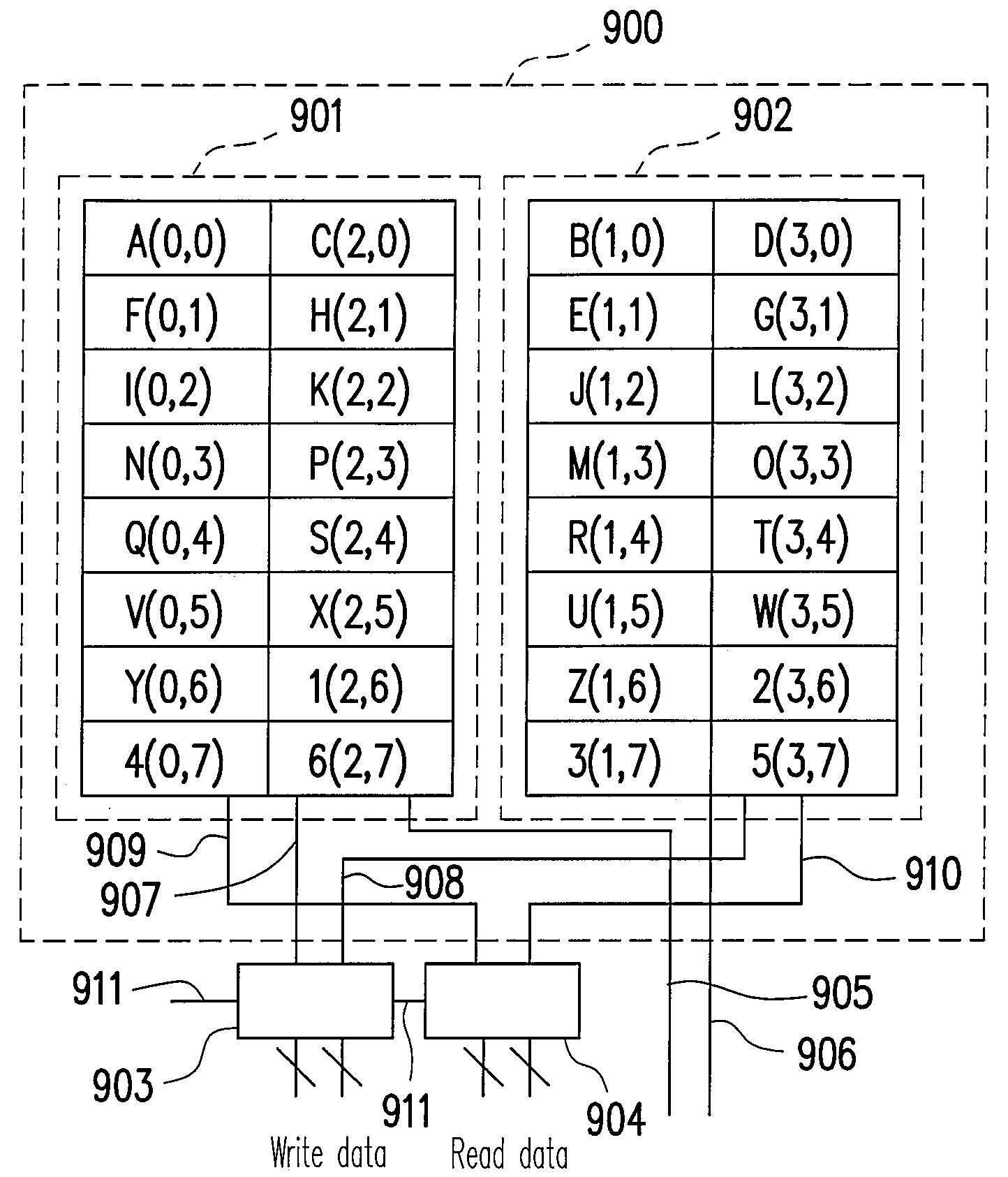
[0041]In the third embodiment, it is required to continuously read and write two batches of data laterally or longitudinally to a memory connected to a display panel. FIG. 3 shows the display panel 300, and data addresses A-Z and 1-6 represent the addresses of the display pixels. FIG. 9 shows a related schematic view of a memory 900 corresponding to the display panel of FIG. 3 after the address conversion. Sub blocks 901 and 902 are two laterally divided sub blocks, and data converters 903 and 904, a left end control signal 905, and a right end control signal 906 are further provided. 907 and 908 respectively represent writing data of the sub blocks 901 and 902, and 909 and 910 respectively represent reading data of the sub blocks 901 and 902. A signal 911 is of a value of Y[0], and it controls data converters 903 and 904, and also controls X[0] value of the right end control signal 906. The data addresses A-Z and addresses 1-6 are addresses after the internal moving of the memory, ...


PUM


Abstract

A method for memory address arrangement is provided. Data of different Y coordinates is moved to operation units divided by different X coordinates, or data of different X coordinates is moved to operation units divided by different Y coordinates, so as to realize the function of simultaneously longitudinally and laterally reading and writing a plurality of batches of data, thereby preventing the limitation of only longitudinally or laterally reading and writing a plurality of batches of data.

Description

CROSS-REFERENCE TO RELATED APPLICATION[0001]This application claims the priority benefit of Taiwan application serial no. 96123772, filed on Jun. 29, 2007. All disclosure of the Taiwan application is incorporated herein by reference.BACKGROUND OF THE INVENTION[0002]1. Field of the Invention[0003]The present invention relates to a method for address arrangement. More particularly, the present invention relates to a method for memory address arrangement.[0004]2. Description of Related Art[0005]As science and technology change quickly, memory develops towards a trend of larger capacity and quicker access speed in correspondence with storage of a large amount of data. The access speed is more required as the memory capacity is larger, and the quicker speed means the higher writing and reading frequency. It is well known that the operation of the memory is mainly writing and reading, so the frequency of writing and reading determines the operating frequency. Therefore, the operating freq...

Claims


Application Information

Patent Timeline
IPC IPC(8): G06F12/06
CPCG11C7/1012G11C7/1006
Inventor LIU, SHANG-I
Owner NOVATEK MICROELECTRONICS CORP
Why Eureka
Try Eureka