
Dram structure and method of making the same

a dram and structure technology, applied in the direction of semiconductor devices, electrical apparatus, transistors, etc., can solve the problems of current leakage and control problems, decrease the operating effect, etc., and achieve the effect of reducing the size, preventing current leakage, and increasing the integration of elements

Active Publication Date: 2009-01-08
NAN YA TECH
View PDF2 Cites 40 Cited by
  • Summary
  • Abstract
  • Description
  • Claims
  • Application Information

AI Technical Summary

Benefits of technology

[0011]The DRAM structure provided in the present invention has a buried word line. Unlike the conventional word line, the buried word line is buried in the substrate rather than being positioned on the surface of the substrate. Therefore, the integration of elements can be increased. In addition, the fin structure can increase the contact area between the control gate and the substrate, so problems of the drain induced barrier lowering (DIBL) effect and the short channel effect can be reduced. Furthermore, the current leakage can be prevented by the conducting strap provided in the present invention. In this way, the DRAM structure can reach a smaller size.

Problems solved by technology

Furthermore, in the conventional DRAM structure, a high electronic field will occur around the junction of the SSBS 218, thereby decreasing the operating effect, and causing current leakage and control problems.

Method used


Image

  • Dram structure and method of making the same
  • Dram structure and method of making the same
  • Dram structure and method of making the same

Examples


first embodiment

[0020]FIG. 2 to FIG. 11 depict a method of making the DRAM structure according to the present invention.

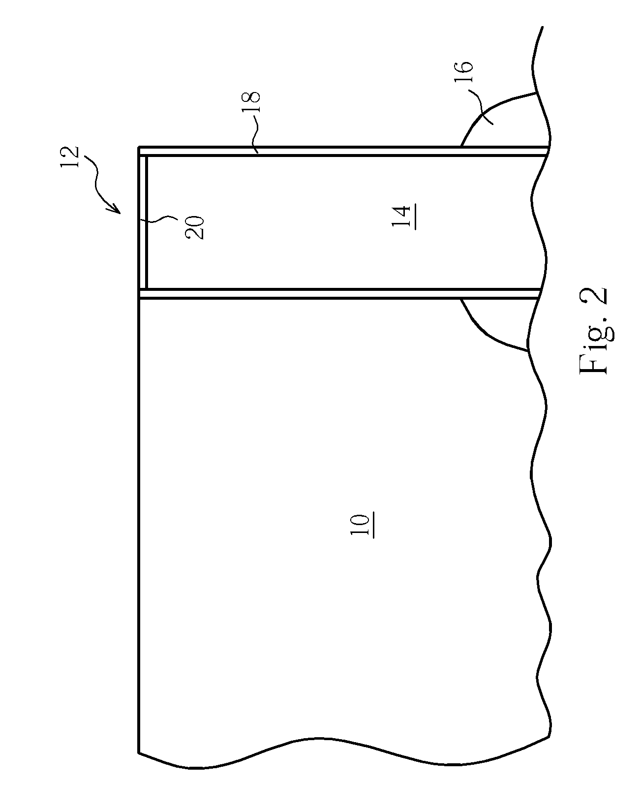
[0021]As shown in FIG. 2, a substrate 10 comprising a first STI structure (not shown) and a trench capacitor 12 is provided. The trench capacitor 12 comprises a conductive layer 14, a bottom electrode 16, and a capacitor dielectric layer 18 surrounding the conductive layer 14 in order to isolate the conductive layer 14 and the substrate 10. A oxide layer 20 is formed on the surface of the conductive layer 14. In the preferred embodiment, the oxide layer 20 is formed coplanar with the substrate 10 surface. The conductive layer 14 can be polysilicon or any conductive materials.

[0022]As shown in FIG. 3, a trench 22 is formed in the substrate 10 and at a side of the trench capacitor 12. As shown in FIG. 4, a oxide layer 24 is formed on the surface of the trench 22 by a thermal or deposition process. The oxide layer serves 24 as an insulation layer. As shown in FIG. 5, a gate matter 26...

second embodiment

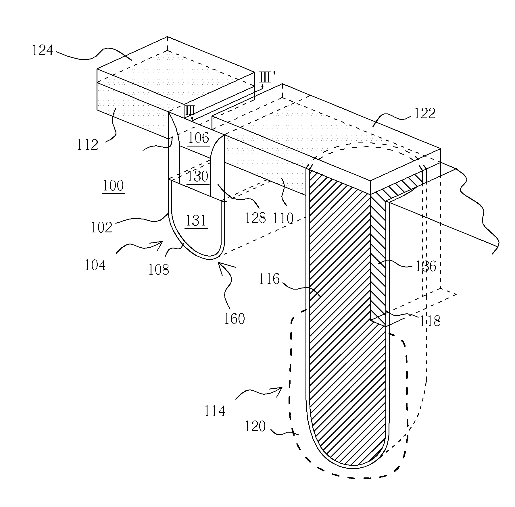
[0044]FIG. 25 shows a sectional view of the DRAM structure of the second embodiment taken along line III-III′ of FIG. 23. As shown in FIG. 25, the buried gate 104 comprises the word line 130, the conductor 131, the cap layer 106, the gate oxide layer 108 (not shown), and the inner spacer 128 (not shown). In addition, the fin structure 132 having an arcuate portion is positioned in the bottom of the trench 102, and the oxide layer 134 serving as an insulating layer covers the surface of the fin structure 132. Due to the formation of the fin structure 132, the oxide layer 134 has an arcuate portion, a fin structure. In this way, the fin structure will become fully depleted during operation, and the DRAM can be controlled more effectively.

[0045]Those skilled in the art will readily observe that numerous modifications and alterations of the device and method may be made while retaining the teachings of the invention.


PUM


Abstract

A DRAM structure has a substrate, a buried transistor with a fin structure, a trench capacitor, and a surface strap on the surface of the substrate. The surface strap is used to electrically connect a drain region to the trench capacitor.

Description

BACKGROUND OF THE INVENTION[0001]1. Field of the Invention[0002]The present invention relates to a DRAM structure and a method of making the same, and more particularly to a DRAM structure that uses a conducting strap to connect a MOS transistor with a trench capacitor. An SSBL (single-sided buried strap) is replaced by the conducting strap. In this way, resistance can be reduced and current leakage can be decreased.[0003]2. Description of the Prior Art[0004]Electrical products are becoming lighter, thinner, shorter, and smaller, and dynamic random access memories (DRAMs) are being scaled down to match the trends of high integration and high density. A DRAM comprising many memory cells is one of the most popular volatile memory devices utilized today. Each memory cell comprises a MOS transistor and at least a capacitor, wherein the MOS transistor and the capacitor form a series connection with each other. By using a word line and a bit line, a DRAM can be read and programmed.[0005]F...

Claims


Application Information

Patent Timeline
Patent Type & Authority Applications(United States)
IPC IPC(8): H01L27/108
CPCH01L27/10823H01L27/10829H01L29/66621H01L29/4236H01L27/10876H10B12/34H10B12/37H10B12/053
Inventor LEE, TZUNG-HANCHENG, CHIH-HAOCHEN, TE-YINLEE, CHUNG-YUANLI, EN-JUI
Owner NAN YA TECH
Features
  • Generate Ideas
  • Intellectual Property
  • Life Sciences
  • Materials
  • Tech Scout
  • Unparalleled Data Quality
  • Higher Quality Content
  • 60% Fewer Hallucinations
Learn More