

Use of discrete conductive layer in semiconductor device to re-route bonding wires for semiconductor device package
a technology of semiconductor devices and conductive layers, applied in the direction of safety/protection circuits, transistors, basic electric elements, etc., can solve the problems of increasing assembly costs, requiring a large amount of effort, and so as to achieve the effect of reducing the performance of mosfet devices and facilitating implementation
- Summary
- Abstract
- Description
- Claims
- Application Information
AI Technical Summary
Benefits of technology
Problems solved by technology
Method used
Image

Examples
Embodiment Construction
[0024]Although the following detailed description contains many specific details for the purposes of illustration, anyone of ordinary skill in the art will appreciate that many variations and alterations to the following details are within the scope of the invention. Accordingly, the exemplary embodiments of the invention described below are set forth without any loss of generality to, and without imposing limitations upon, the claimed invention.
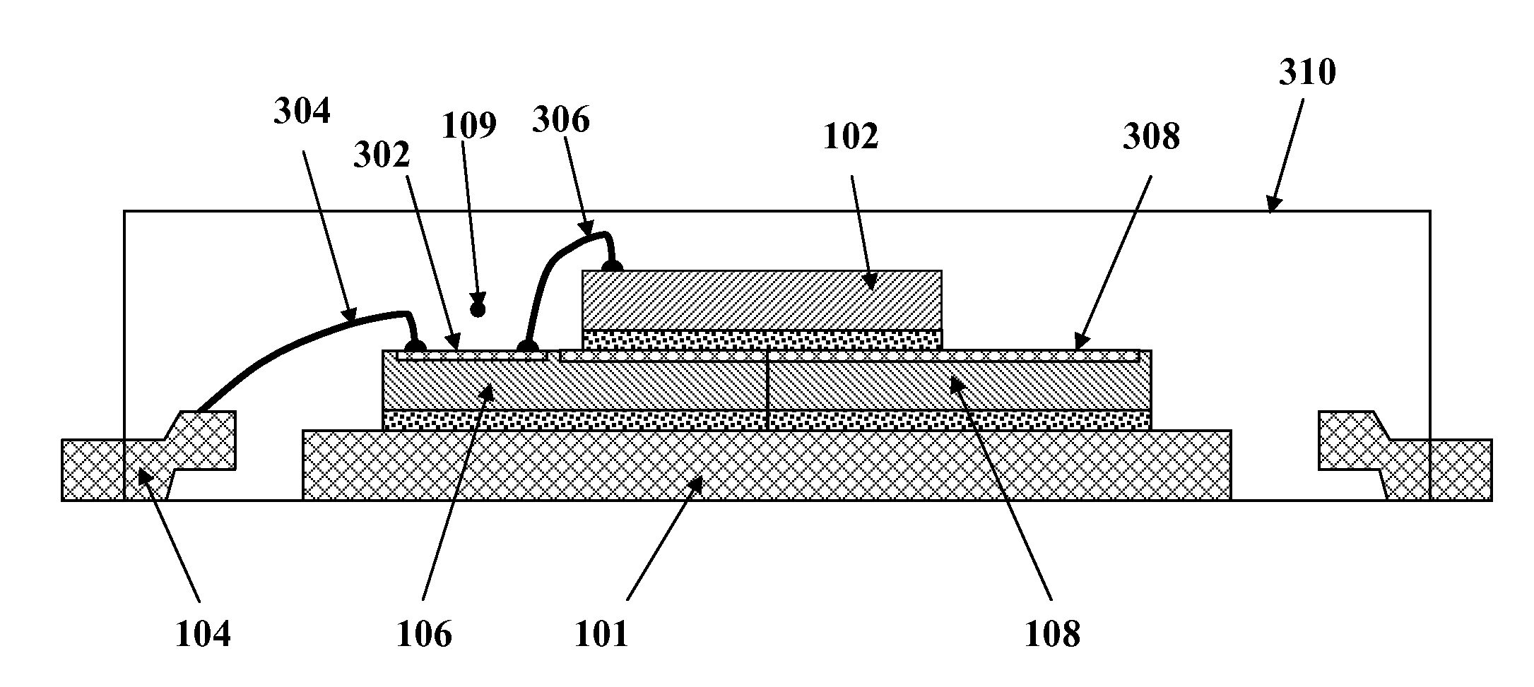
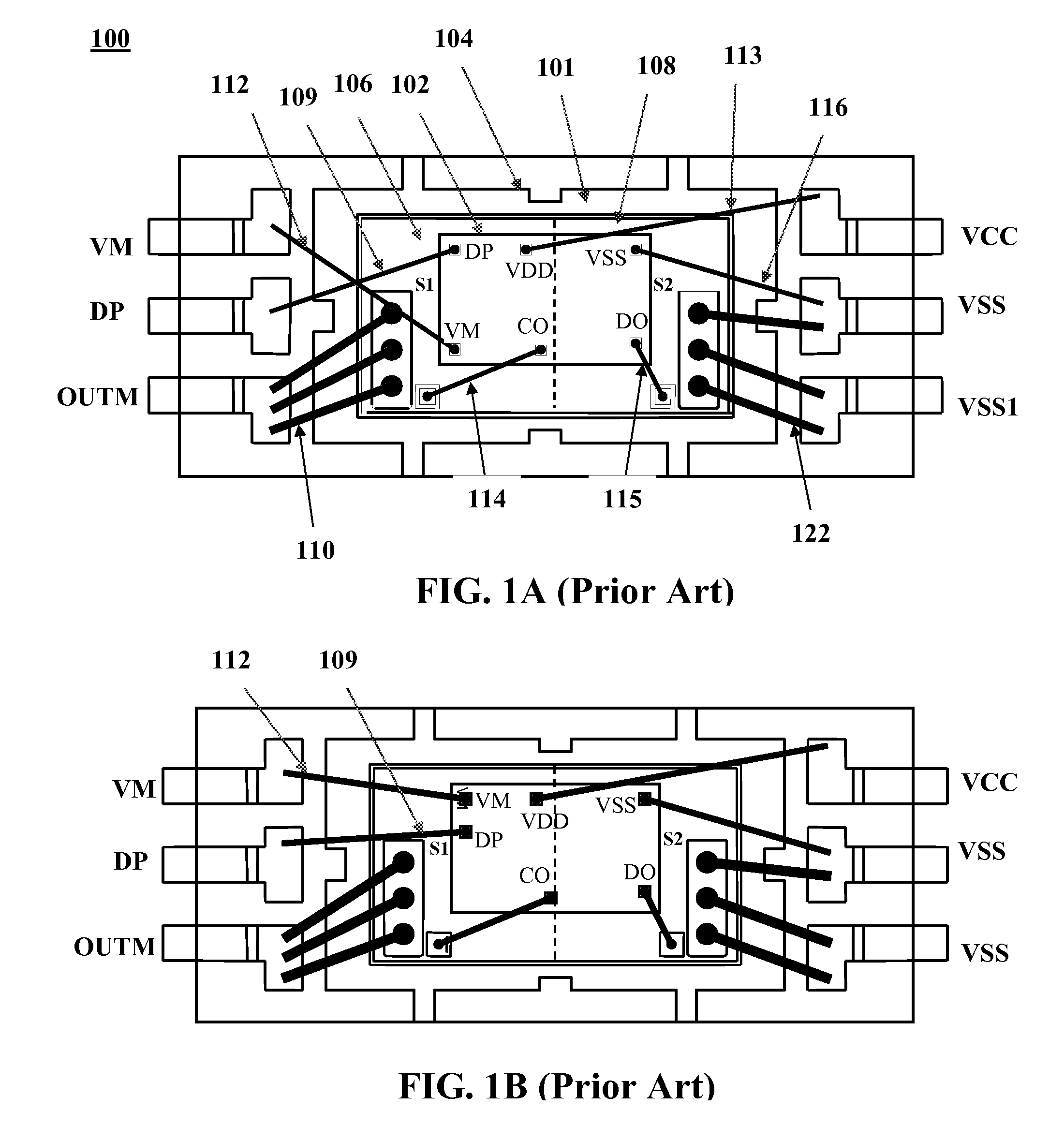
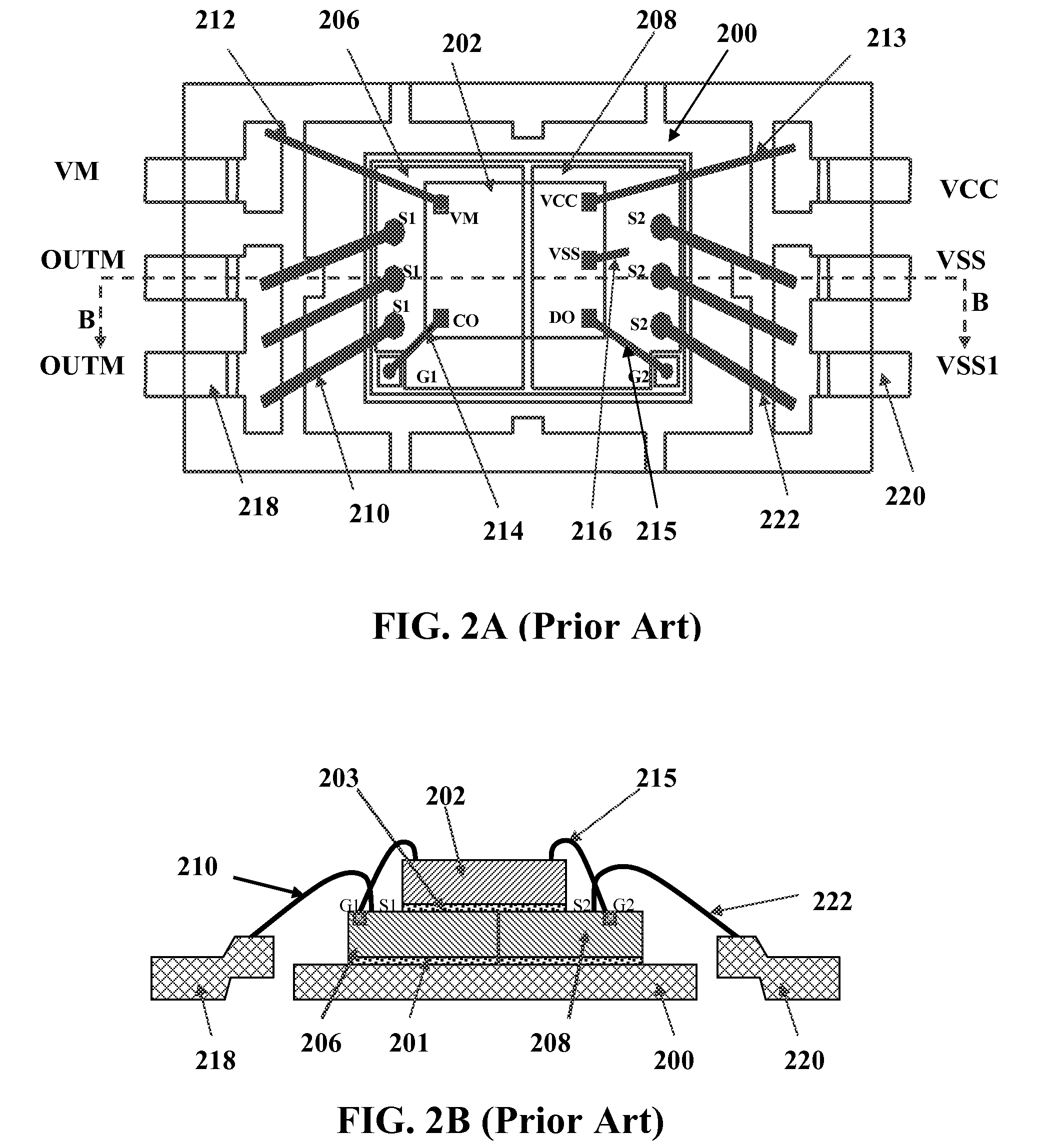
[0025]Embodiments of the present invention overcome the above-described problems through the use of a semiconductor device that includes an electrically isolated conductive trace formed from a layer of conductive material in the top portion of the device. The conductive trace may be configured to provide an electrically conductive path between a first bond wire and a second bond wire. The conductive path may pass underneath a third bond wire thereby avoiding a situation where the third bond wire crosses with another bond wire. A bond wire wh...
PUM
 Abstract
Description
Claims
Application Information