Magnetoresistive random access memory

a random access and memory technology, applied in the field of magnetic random access memory, can solve the problems of increasing the power consumption of mram and the small area available for providing memory cells, and achieve the effect of low resistance state and high resistance sta

Active Publication Date: 2009-01-08
KIOXIA CORP
View PDF6 Cites 32 Cited by
  • Summary
  • Abstract
  • Description
  • Claims
  • Application Information

AI Technical Summary

Benefits of technology

[0011]According to an aspect of the present invention, there is provided a magnetoresistive random access memory comprising: a first magnetoresistive effect element that takes a low resistance state and a high resistance state; a second magnetoresistive effect element fixed to a low resistance state or a high resistance state; a first MOSFET having a first end connected to the first magnetoresistive effect element and having a gate terminal that receives first potential; a second MOSFET having a first end connected to the second magnetoresistive effect element; a sense amplifier amplifying a difference between a value of current that flows through a second end of the first MOSFET and a value of current that flows through a second end of the second MOSFET; a current circuit outputting reference current whose value lies between current that flows through the first magnetoresistive effect element of the low resistance state and current that flows through the first magnetoresistive effect element of the high resistance state; a third MOSFET having a first end that receives the reference current and is connected to its own gate terminal, a gate terminal of the second MOSFET receiving substantially the same potential as the gate terminal of the third MOSFET; and a first resistance element connected to a second end of the third MOSFET and having substantially the same resistance as the second magnetoresistive effect element.

Problems solved by technology

However, this method requires more than one reference cells to generate one reference signal.
Therefore, the cramp circuits, which are big due to operational amplifiers, occupy a large area of MRAM, resulting in smaller area available for providing memory cells.
For this reason, the operational amplifiers that need current flowing through them at the time of operation increase the power consumption of MRAM.

Method used


Image

  • Magnetoresistive random access memory
  • Magnetoresistive random access memory
  • Magnetoresistive random access memory

Examples


first embodiment

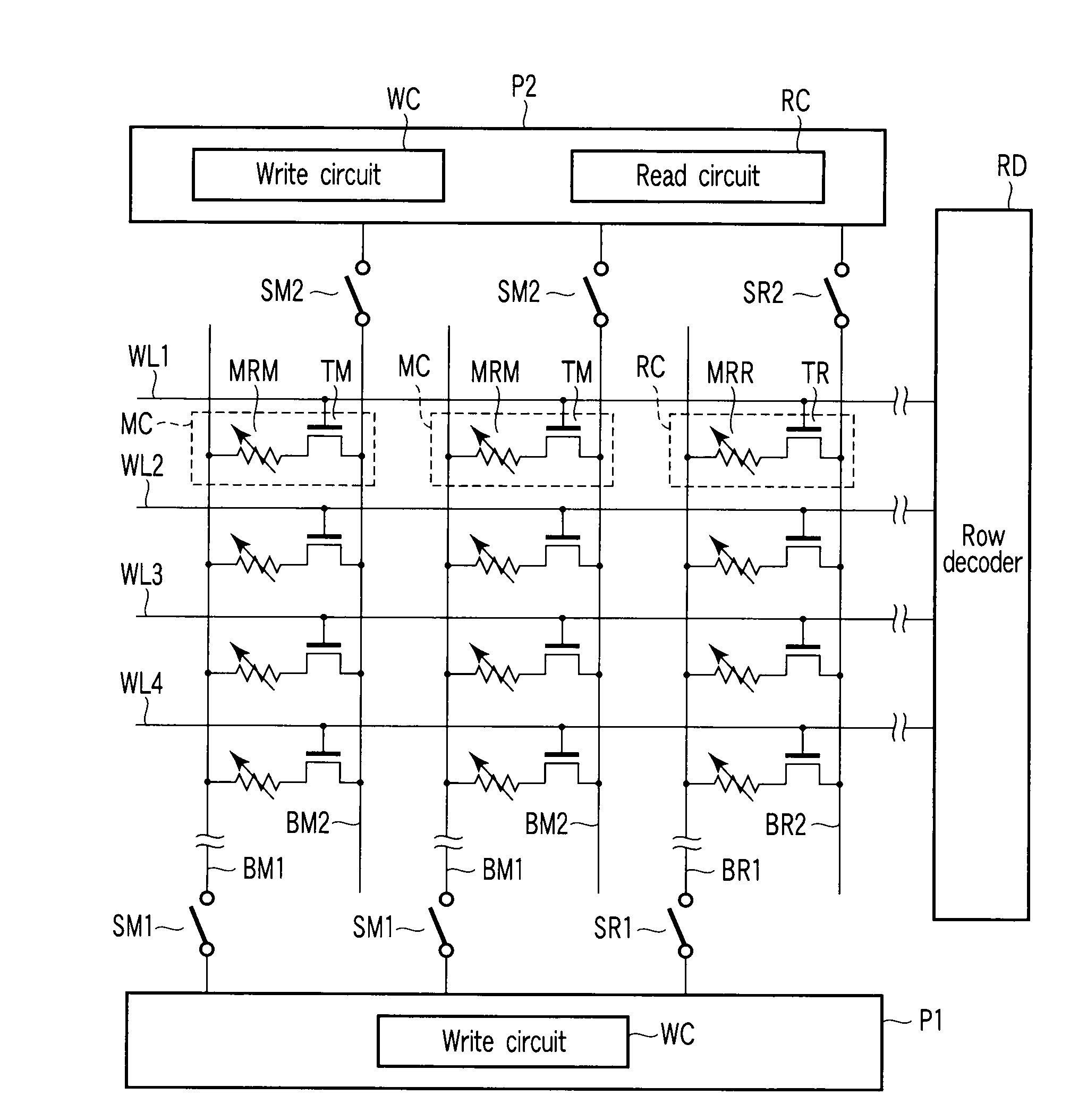
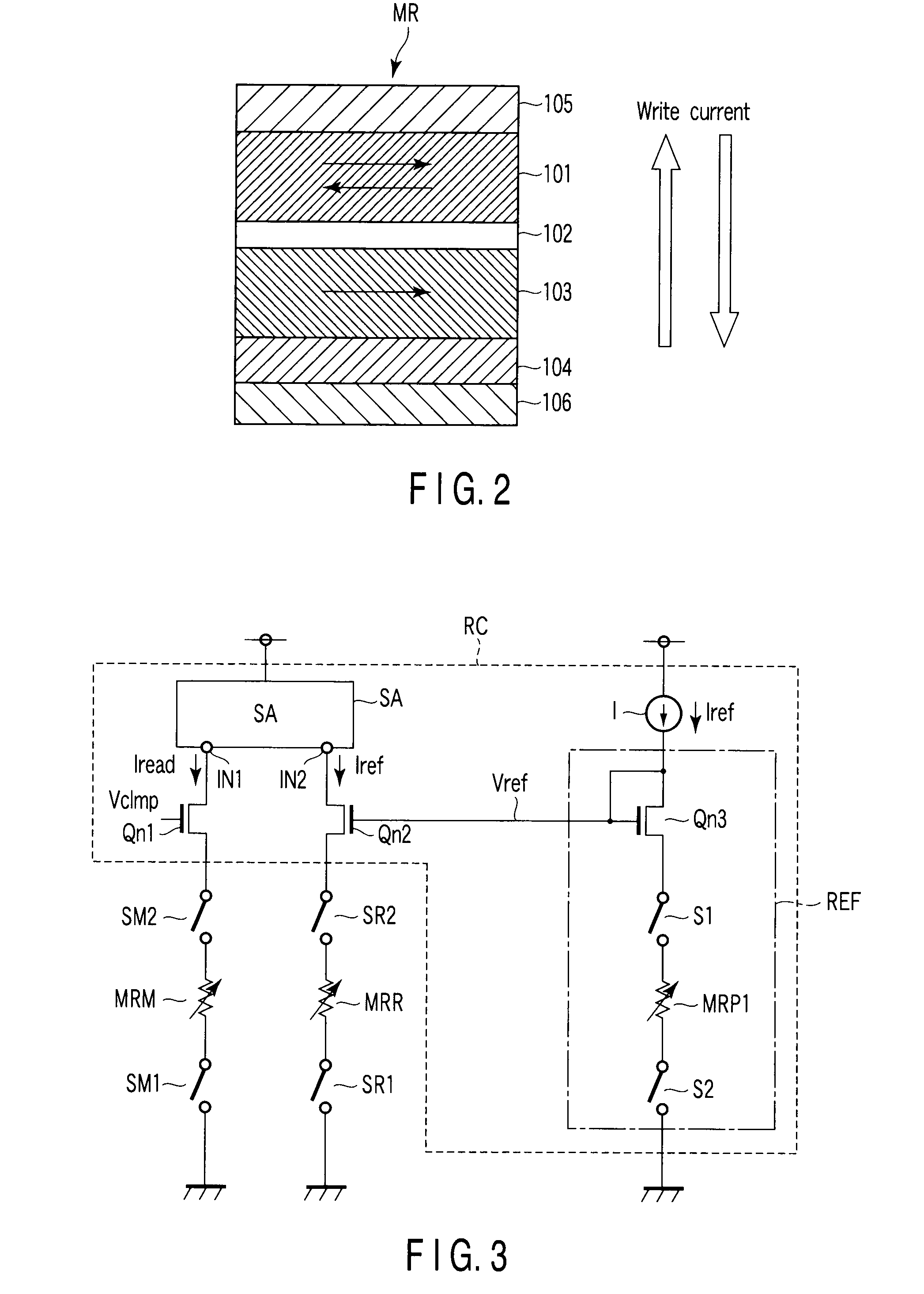
[0021]With reference to FIGS. 1 to 3, the magnetoresistive random access memory according to the first embodiment of the present invention is explained. FIG. 1 is a circuit diagram schematically showing main parts of the magnetoresistive random access memory according to the first embodiment. As shown inFIG. 1, memory cells MC and reference cells RC are arranged in a matrix. The memory cell MC consists of a magnetoresistive effect (MR) element MRM and a select transistor TM that are connected in series. The reference cell RC consists of a MR element MRR and a select transistor TR that are connected in series. Select transistors TM and TR consist of, for example, n-type metal oxide semiconductor field effect transistor (MOSFET).

[0022]MR elements MRM and MRR can take at least two stationary states in accordance with its internal magnetization state. More specifically, MR elements MRM and MRR are designed to take a low resistance state or a high resistance state when flow of spin-polar...

second embodiment

[0059]The second embodiment concerns the connection between transistors Qn2 and Qn3. FIG. 4 is a circuit diagram schematically showing main parts of the magnetoresistive random access memory according to the second embodiment of the present invention. As shown in FIG. 4, in read circuit RC, the potential of the gate terminal of transistor Qn3 is transmitted to the gate terminal of transistor Qn2 through a unity gain buffer.

[0060]Specifically, the gate terminal of transistor Qn3 is connected to the non-reversed input terminal of an operational amplifier OP. The output terminal of operational amplifier OP is connected to the gate terminal of transistor Qn2 and its own reversed input terminal. Even if transistors Qn2 and QN3 are connected in this way, gate terminals of transistor Qn2 and Qn3 can have the same potential. The remaining parts are the same as the first embodiment.

[0061]Connecting gate terminals of transistor Qn2 and QN3 through operational amplifier OP can charge the gate ...

third embodiment

[0064]The third embodiment concerns the example of constant current circuit I of first and second embodiments.

[0065]FIG. 5 is a circuit diagram schematically showing main parts of read circuit RC of the magnetoresistive random access memory according to the third embodiment of the present invention. Constant current circuit I has the configuration shown in FIG. 5.

[0066]As shown in FIG. 5, in constant current circuit I, p-type MOSFET Qp1, an n-type MOSFET Qn11, and a replica MR element MRP2 are serially connected. The serially-connected structure is connected between the power supply potential end and the common potential end. The gate terminal of transistor Qp1 is connected to the drain terminal thereof. Clamp potential Vclmp is supplied to the gate terminal of transistor Qn11.

[0067]In constant current circuit I, a p-type MOSFET Qp2, an n-type MOSFET Qn13, and a replica MR element MRP3 are serially connected. The serially-connected structure is connected between the power supply pot...


PUM


Abstract

A MRAM includes a first magnetoresistive effect (MR) element that takes a low and high resistance states. A second MR element is fixed to a low or high resistance state. First and second MOSFETs are connected to the first and second MR elements, respectively. A sense amplifier amplifies a difference between values of current flowing through the first and second MOSFETs. A current circuit outputs reference current whose value lies between current flowing through the first MR element of the low and high resistance states. A third MOSFET has one end that receives the reference current and is connected to its own gate terminal. The gate terminal of the second MOSFET receives the same potential as the gate terminal of the third MOSFET. A first resistance element is connected to the others end of the third MOSFET and has the same resistance as the second magnetoresistive effect element.

Description

CROSS-REFERENCE TO RELATED APPLICATIONS[0001]This application is based upon and claims the benefit of priority from prior Japanese Patent Application No. 2007-175564, filed Jul. 3, 2007, the entire contents of which are incorporated herein by reference.BACKGROUND OF THE INVENTION[0002]1. Field of the Invention[0003]The present invention relates to a magnetoresistive random access memory, in particular, for example, the read circuit configuration of the magnetoresistive random access memory.[0004]2. Description of the Related Art[0005]Magnetoresistive random access memory (MRAM) is the nonvolatile memory that can be accessed high-speed. MRAM uses magnetoresistive effect (MR) elements to store information. A MR element takes two different resistance, corresponding to the state of magnetization. Reading is performed by distinguishing the resistance of MR elements. Therefore, the reading method of detecting the resistance of the MR element with sufficient accuracy is needed.[0006]One of...

Claims


Application Information

Patent Timeline
Patent Type & Authority Applications(United States)
IPC IPC(8): G11C11/02
CPCG11C11/15G11C11/1673
Inventor UEDA, YOSHIHIRO
Owner KIOXIA CORP
Why Eureka
Try Eureka