Electron beam apparatus

a technology of electron beam and apparatus, which is applied in the direction of material analysis using wave/particle radiation, instruments, nuclear engineering, etc., can solve the problems of significant limit the precision of sample evaluation, and achieve the effect of reducing aberration and high-precision image data

Inactive Publication Date: 2009-01-15
KK TOSHIBA
View PDF52 Cites 48 Cited by
  • Summary
  • Abstract
  • Description
  • Claims
  • Application Information

AI Technical Summary

Benefits of technology

[0024]According to the present invention, the above-mentioned structure is employed, and the following advantages are obtained.
[0025]The auxiliary lens is provided in the image plane located on the incident side of the axial chromatic aberration correction lens, so that abaxial aberration caused by the axial chromatic aberration correction lens can be reduced. Therefore, it is possible to obtain high-precision image data whose aberration is reduced.
[0026]In the multibeam type electron beam device, regardless of whether the angle formed between the beam arrangement direction and the reference coordinate axis is appropriate, and regardless of whether the beam interval is equal to a predetermined value can be evaluated based on an interval between the obtained signals, so that the angle and the beam interval can be precisely adjusted.

Problems solved by technology

Factors which may significantly limit precision of evaluation of a sample when using an electron beam device are caused by axial chromatic aberrations and spherical aberrations.

Method used


Image

  • Electron beam apparatus
  • Electron beam apparatus
  • Electron beam apparatus

Examples


first embodiment

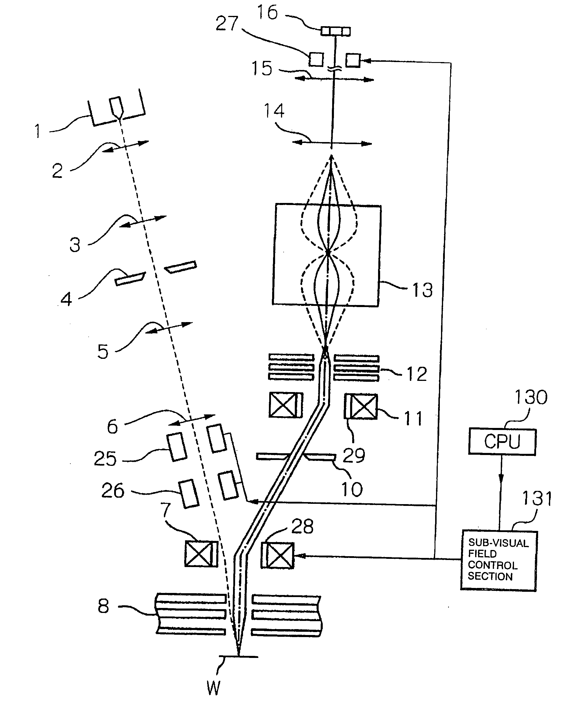
[0039]FIG. 1 shows a principal part of an electron beam device using a mapping projection type electronic optical system according to the present invention. In the electron beam device, an irradiation region size and an irradiation current density of an electron beam emitted from an electron gun 1 are adjusted by two stages of condenser lenses 2 and 3. The electron beam is formed to rectangular by a rectangular aperture 4 which is square or rectangular in shape. The magnification of a shaped rectangular primary electron beam is adjusted by two stages of irradiation lenses 5 and 6. A sub-visual field within a rectangular visual field on a sample W is irradiated with the electron beam passing through a beam separator 7 and an objective lens 8. The visual field on the sample W is divided into, for example, nine sub-visual fields arranged in a scanning direction of the primary electron beam. Selecting the sub-visual fields is performed by electrostatic deflectors 25 and 26. Irradiation ...

second embodiment

[0061]FIG. 4 shows an electron beam device according to the present invention. The electron beam device uses a mapping projection type electronic optical system and includes a primary electron optical system 100 for forming a rectangular beam from an electron beam emitted from an electron gun 51 and focusing the rectangular beam on the sample W, a secondary electron optical system 200 for magnifying an image of secondary electrons emitted from a surface of the sample W, a detection device 300 for detecting the secondary electrons injected from the secondary electron optical system, a voltage control power supply 400 which is a variable voltage source, and a control device 500 for controlling the entire electron beam device.

[0062]The primary electron optical system 100 includes the electron gun 51 having an LaB6 cathode for emitting a primary electron beam, a condenser lens 53 for focusing the primary electron beam emitted from the electron gun 51, a shaping aperture portion 55 for s...

third embodiment

[0090]As described above, according to the electron beam device in the present invention, the high voltage is applied to the cylindrical electrode 644 of the objective lens 642, so that the axial chromatic aberration can be reduced to a small value. Since the magnetic pole 675 is in substantially a ground state, it is possible to prevent discharge between the cylindrical electrode 644 and the sample W, even when the high voltage is applied to the cylindrical electrode 644. The voltage applied to the cylindrical electrode 644 can be adjusted by the voltage control power supply 400′, so the absolute value of the positive axial chromatic aberration which is caused by the objective lens 642 can be made equal to the absolute value of the negative axial chromatic aberration which is caused by the chromatic aberration correction lens 37. Therefore, the axial chromatic aberration can be reliably corrected. As a result, the residual chromatic aberration is small, so the angular aperture can ...


PUM

PropertyMeasurementUnit
lengthaaaaaaaaaa
transmittanceaaaaaaaaaa

Abstract

Secondary electrons emitted from a sample (W) by an electron beam irradiation is deflected by a beam separator (77), and is deflected again in a perpendicular direction by an aberration correction electrostatic deflector (711) to form a magnified image on the principal plane of an auxiliary lens (712). The secondary electron beam diverged from the auxiliary lens (712) passes through axial chromatic aberration correction lenses (714-717) and images on a principal plane of an auxiliary lens (718) for a magnifying lens (719). The magnified image is formed in a position spaced apart from the optical axis. Therefore, when the secondary electron beam diverged from the auxiliary lens (712) is incident on the axial chromatic aberration correction lenses without any change, large abaxial aberration occurs. To avoid it, the auxiliary lens (712) is used to form the image of an NA aperture (724) in substantially a middle (723) in the light axis direction of the axial chromatic aberration correction lenses (714-717).

Description

TECHNICAL FIELD[0001]The present invention relates to an electron beam device. More particularly, the present invention relates to an electron beam device, which irradiates a sample with an electron beam and detects with a detector, electrons emitted from the sample upon irradiation of the sample with the electron beam, whereby evaluation of defects and the like of the sample can be achieved with high throughput and reliability.BACKGROUND ART[0002]Factors which may significantly limit precision of evaluation of a sample when using an electron beam device are caused by axial chromatic aberrations and spherical aberrations.[0003]There is used with respect to an SEM electron beam device, and a transmission electron microscope (TEM), a device having a Wien filter and / or a quadrupole lens, which is capable of correcting axial chromatic aberration.[0004]There is also used an electron beam device in which an electrostatic lens is used as an objective lens, and a high voltage is applied to ...

Claims


Application Information

Patent Timeline
Patent Type & Authority Applications(United States)
IPC IPC(8): G01N23/00
CPCH01J37/153H01J37/26H01J2237/28H01J2237/2446H01J2237/1534H01J37/10
Inventor NAKASUJI, MAMORUNOJI, NOBUHARUSATAKE, TOHRUKAGA, TORUSOBUKAWA, HIROSIMURAKAMI, TAKESHIKARIMATA, TSUTOMU
Owner KK TOSHIBA
Why Eureka
Try Eureka