

Semiconductor device with large blocking voltage
a technology of blocking voltage and semiconductor, applied in the direction of semiconductor devices, electrical devices, transistors, etc., can solve the problems of voltage exceeding, low threshold voltage, gate voltage for turning on the element, etc., and achieve the effect of large gate noise margin
- Summary
- Abstract
- Description
- Claims
- Application Information
AI Technical Summary
Benefits of technology
Problems solved by technology
Method used
Image

Examples
first embodiment
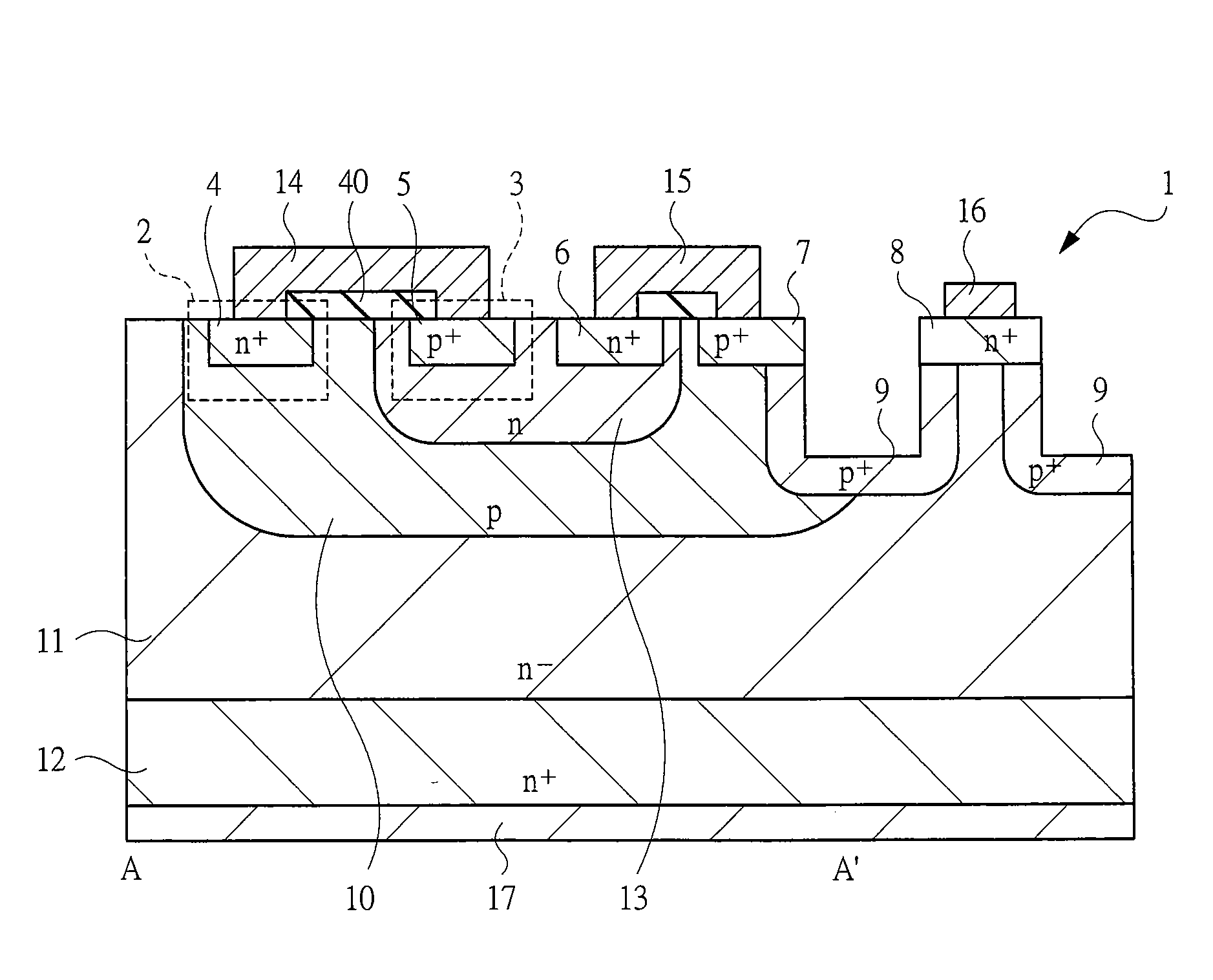
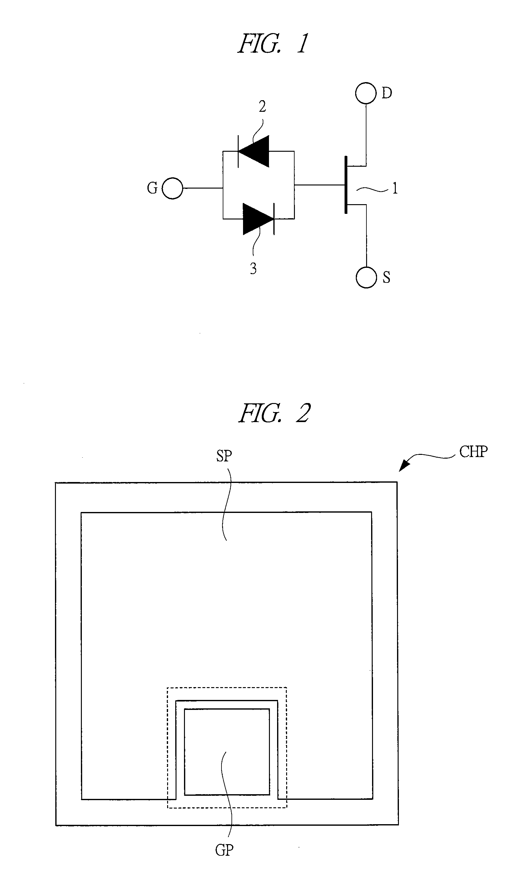
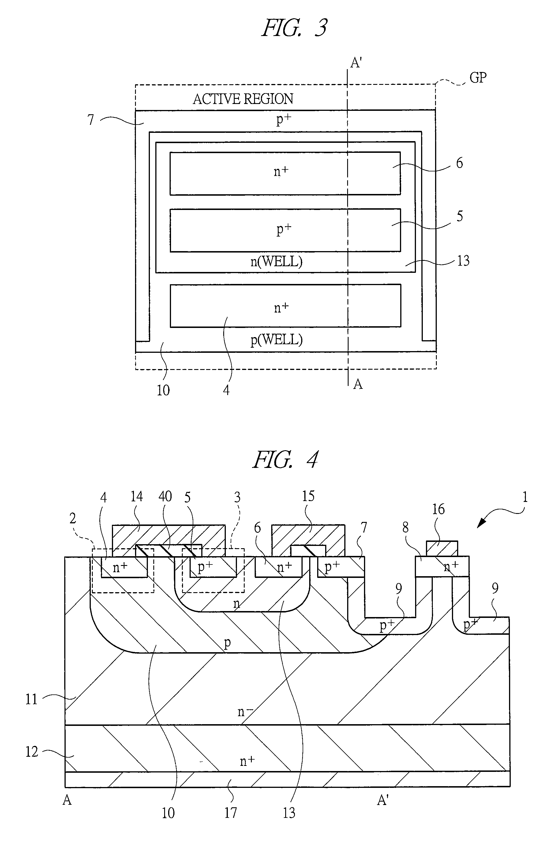
[0045]First, in a first embodiment, a semiconductor device having a junction FET as a gate-controlled type semiconductor element (a switching element, a transistor) will be described with reference to FIGS. 1 to 4. FIGS. 1 to 4 are an equivalent circuit diagram of, a plan view of, a plan view showing essential parts of, and a cross-sectional view showing essential parts of the semiconductor device according to the first embodiment, respectively. FIG. 2 shows the semiconductor device as a chip (CHP), and a gate pad GP and a source pad SP are formed over the chip CHP. FIG. 3 is a plan view of a region of the gate pad GP in FIG. 2 from which the gate pad GP is removed. A cross-sectional view taken along a line A-A′ in FIG. 3 is shown in FIG. 4. Note that, in this application, the gate pad GP is sometimes referred to as a gate electrode, and the source pad SP is sometimes referred to as a source electrode. And, as shown in FIG. 4, a drain electrode 17 is formed as a back surface electro...
second embodiment
[0067]In a second embodiment of the present invention, a semiconductor device comprising a junction FET as a gate-controlled type semiconductor element (a switching element, a transistor) is described with reference to FIGS. 13 and 14. FIGS. 13 and 14 are an equivalent circuit diagram of and a cross-sectional view showing essential parts of the semiconductor device according to the second embodiment, respectively.
[0068]As shown in FIGS. 13 and 14, the semiconductor device according to the second embodiment differs from the semiconductor device according to the first embodiment in that the diode in the reverse direction in the diode portion is not the pn diode 2 but a Schottky barrier diode 18. As shown in FIG. 14, the Schottky barrier diode 18 is formed by forming a Schottky metal 19 of metal contacting with the p well 10 to make junction having a rectification property with the p well 10 after the p well 10, which is a semiconductor region, is formed.
[0069]The Schottky barrier diod...
third embodiment
[0070]In a third embodiment, a semiconductor device comprising a MISFET as a gate-controlled type semiconductor element (a switching element, a transistor) is described with reference to FIGS. 15 to 17. FIGS. 15 and 16 are a plan view showing essential parts of and a cross-sectional view showing essential parts of the semiconductor device according to the third embodiment, respectively. FIG. 15 is a plan view of the region of the gate pad GP shown in FIG. 2, for example, from which the gate pad GP is removed. A cross-sectional view taken along a line B-B′ in FIG. 15 is shown in FIG. 16. FIG. 17 shows a circuit diagram in a case where the semiconductor device according to the third embodiment is applied to an inverter circuit.
[0071]As shown in FIGS. 15 and 16, the semiconductor device according to the third embodiment comprises a MISFET (see FIG. 26, for example) and a diode portion incorporated in the region of the gate pad GP shown in FIG. 2, for example. A pn diode 2 in a reverse ...
PUM
 Abstract
Description
Claims
Application Information