Manufacturing process and structure of through silicon via

a manufacturing process and silicon via technology, applied in the direction of semiconductor devices, semiconductor/solid-state device details, electrical apparatus, etc., can solve the problems of deteriorating yield, increasing the inductance between wirings, and difficult high-speed transmission

Inactive Publication Date: 2009-01-15
RENESAS ELECTRONICS CORP
View PDF5 Cites 130 Cited by
  • Summary
  • Abstract
  • Description
  • Claims
  • Application Information

AI Technical Summary

Benefits of technology

[0010]In recent years, the development of SiP (System in Package) in which a plurality of semiconductor chips are mounted densely to realize a high-performance system in a short term has been in progress, and various mounting structures have been proposed by various manufacturers. In particular, SiP in which a plurality of chips are three-dimensionally stacked has an advantage in a mounting area.

Problems solved by technology

Accordingly, the inductance between wirings increases and high-speed transmission becomes difficult, and further, yield is deteriorated due to the increase in density of the wirings formed on the mounting board and the cost increase of a semiconductor device is caused.

Method used


Image

  • Manufacturing  process and structure of through silicon via
  • Manufacturing  process and structure of through silicon via
  • Manufacturing  process and structure of through silicon via

Examples


first embodiment

[0071]In the first embodiment, the description will be made with reference to the drawings with using a semiconductor device in which a highly integrated circuit is mounted like a microcomputer chip as an example.

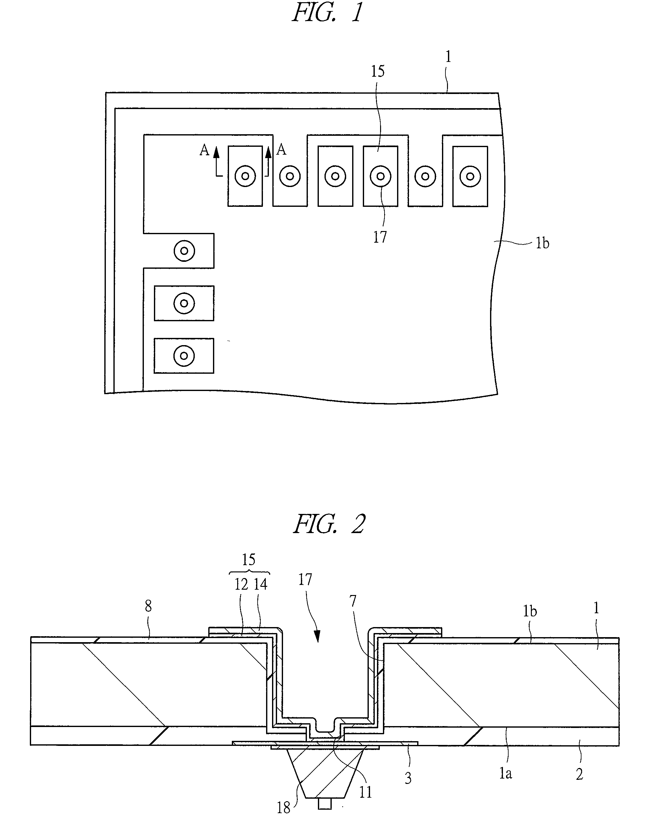
[0072]FIG. 1 is a plan view showing a semiconductor chip according to the first embodiment. FIG. 1 is a drawing showing a part of a semiconductor chip on a side of a second surface (rear surface) 1b of a semiconductor substrate 1 seen from above. As shown in FIG. 1, the semiconductor chip is constituted of the semiconductor substrate 1 of a rectangular shape, and a plurality of through silicon vias 17 are formed in the second surface 1b of the semiconductor substrate 1. Also, the plurality of through silicon vias 17 are connected to wirings formed of a conductive film 15, and a wiring pattern is formed by these wirings on the second surface 1b of the semiconductor substrate 1. As mentioned above, in the first embodiment, the plurality of through silicon vias 17 are formed i...

second embodiment

[0129]Although the semiconductor chip in which a highly integrated circuit is formed like a microcomputer chip has been described in the first embodiment, a semiconductor chip for performing the rewiring like an interposer chip will be described in the second embodiment.

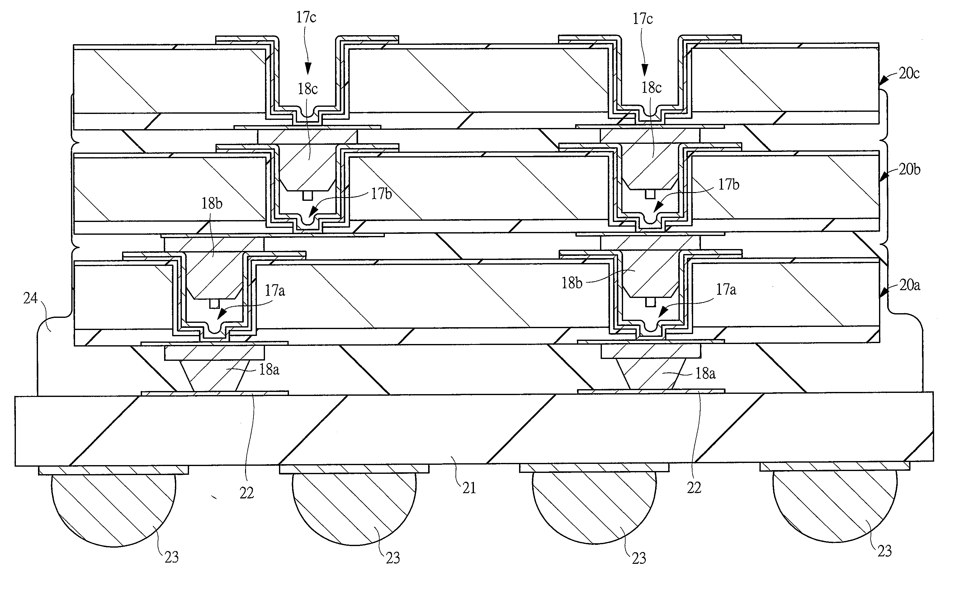
[0130]For example, when a plurality of semiconductor chips are three-dimensionally stacked, a stud bump electrode formed in a semiconductor chip disposed above is deformed and inserted into a through silicon via formed in a semiconductor chip disposed below, thereby electrically connecting the upper and lower semiconductor chips. At this time, respectively different integrated circuits are formed in the semiconductor chip disposed above and the semiconductor chip disposed below, and they have different functions in many cases. Thus, the upper and lower semiconductor chips have different layout patterns, respectively. Accordingly, the position of the through silicon via of the semiconductor chip disposed below and the...

third embodiment

[0137]Although an example of using the insulating film 8 has been described in the first embodiment, an example of using a photosensitive insulating film instead of the insulating film 8 will be described in the third embodiment. The manufacturing method of a semiconductor chip in the third embodiment will be described below.

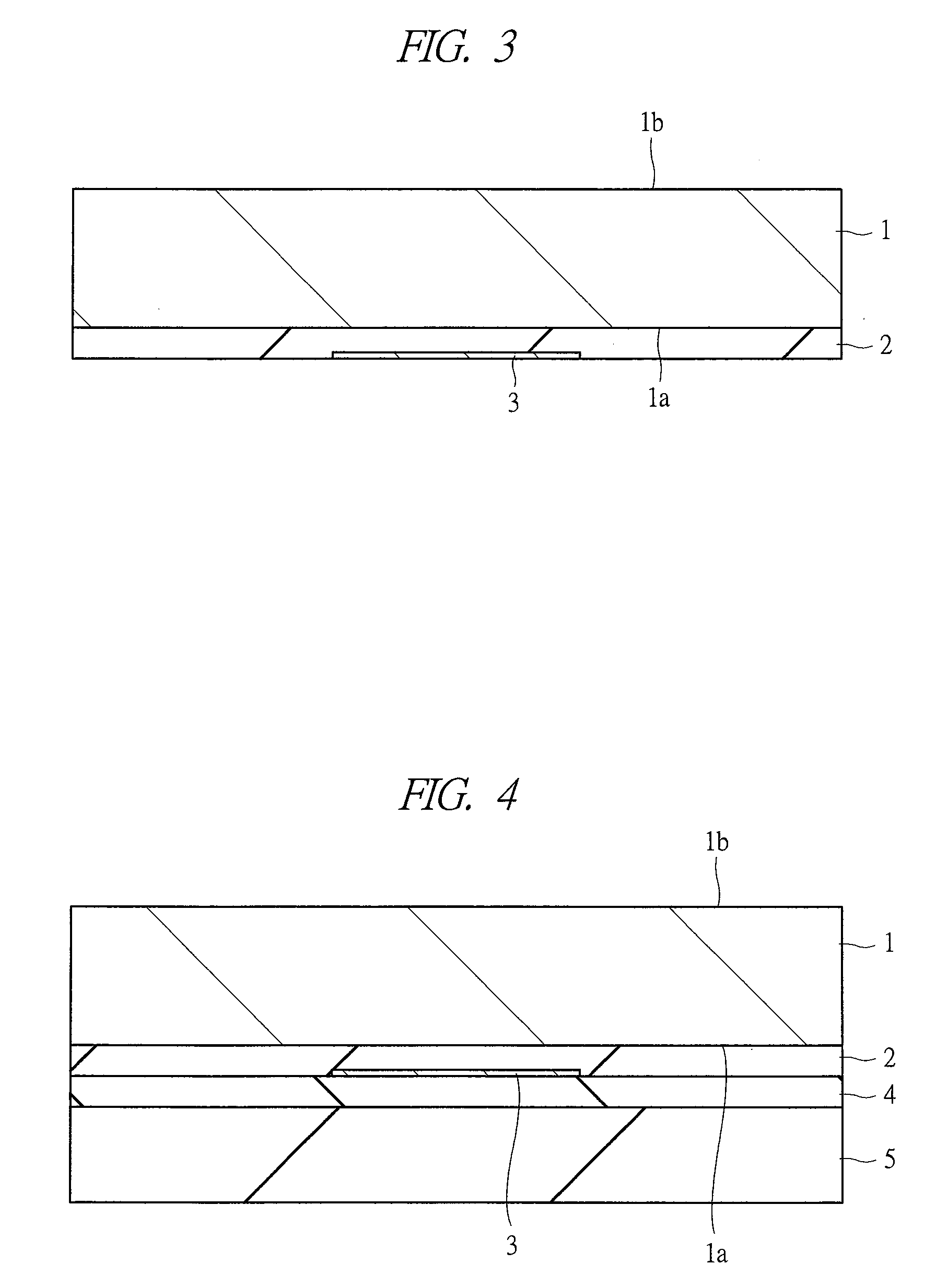
[0138]By performing the process shown from FIG. 3 to FIG. 7, the first hole 7 which reaches the interlayer insulating film 2 from the second surface 1b of the semiconductor substrate 1 is formed. Then, as shown in FIG. 38, after removing the resist film 6, the interlayer insulating film 2 exposed on the bottom surface of the first hole 7 is etched to the middle with using the semiconductor substrate 1 made of silicon and the first hole 7 formed in the semiconductor substrate 1 as a mask.

[0139]Then, as shown in FIG. 39, a photosensitive insulating film 8a is formed on the second surface 1b of the semiconductor substrate 1 including the inside of the first hole 7....


PUM


Abstract

A through silicon via reaching a pad from a second surface of a semiconductor substrate is formed. A penetration space in the through silicon via is formed of a first hole and a second hole with a diameter smaller than that of the first hole. The first hole is formed from the second surface of the semiconductor substrate to the middle of the interlayer insulating film. Further, the second hole reaching the pad from the bottom of the first hole is formed. Then, the interlayer insulating film formed on the first surface of the semiconductor substrate has a step shape reflecting a step difference between the bottom surface of the first hole and the first surface of the semiconductor substrate. More specifically, the thickness of the interlayer insulating film between the bottom surface of the first hole and the pad is smaller than that in other portions.

Description

CROSS-REFERENCE TO RELATED APPLICATION[0001]The present application claims priority from Japanese Patent Application No. JP 2007-150289 filed on Jun. 6, 2007, the content of which is hereby incorporated by reference into this application.TECHNICAL FIELD OF THE INVENTION[0002]The present invention relates to a semiconductor device and a manufacturing technology thereof. More particularly, it relates to a technology effectively applied to a semiconductor device having a plurality of semiconductor chips stacked three-dimensionally and a manufacturing technology of the semiconductor device.BACKGROUND OF THE INVENTION[0003]Japanese Patent Application Laid-Open Publication No. 11-204720 (Patent Document 1) discloses a technology in which an electrical connection between stacked semiconductor chips is made by wire bonding in a three-dimensional stacking type SiP (System in Package).[0004]Japanese Patent Application Laid-Open Publication No. 2000-260934 (Patent Document 2) discloses a techn...

Claims


Application Information

Patent Timeline
Patent Type & Authority Applications(United States)
IPC IPC(8): H01L23/52H01L21/60H01L21/4763
CPCH01L21/6835H01L21/76898H01L2924/0002H01L24/05H01L2924/1306H01L2224/05553H01L2224/05572H01L2224/0557H01L2224/05025H01L24/90H01L25/0657H01L25/50H01L2221/68372H01L2224/0401H01L2224/1134H01L2224/13025H01L2224/13099H01L2224/90H01L2225/06513H01L2225/06517H01L2225/06541H01L2924/01002H01L2924/01004H01L2924/01005H01L2924/01013H01L2924/01014H01L2924/01015H01L2924/01018H01L2924/01022H01L2924/01029H01L2924/01033H01L2924/01047H01L2924/01078H01L2924/01079H01L2924/01082H01L2924/014H01L2924/04941H01L2924/05042H01L2924/14H01L2924/30107H01L2924/00013H01L2924/01006H01L2924/01019H01L2924/01024H01L2224/16147H01L2224/16237H01L2224/81191H01L2224/81141H01L2924/00014H01L2924/00H01L2224/05552H01L2224/023H01L2924/0001H01L23/12H01L23/48
Inventor KAWASHITA, MICHIHIROYOSHIMURA, YASUHIROTANAKA, NAOTAKANAITO, TAKAHIROAKAZAWA, TAKASHI
Owner RENESAS ELECTRONICS CORP
Why Eureka
Try Eureka