Variable transconductance circuit

a transconductance circuit and variable technology, applied in differential amplifiers, amplifiers with semiconductor devices/discharge tubes, amplifiers, etc., can solve problems such as increased current consumption, low power supply voltage operation is therefore difficult, and problems in current consumption and on-board circuit area, so as to reduce the amount of current change required for varying gm, high gm, and low power consumption

Active Publication Date: 2009-01-15
PANASONIC SEMICON SOLUTIONS CO LTD
View PDF9 Cites 5 Cited by
  • Summary
  • Abstract
  • Description
  • Claims
  • Application Information

AI Technical Summary

Benefits of technology

[0020]The first effect is that a variable gm circuit permitting a wide range of variation with a low power supply voltage can be attained in a small scale. The reason for this is that the current change amount required for varying gm can be reduced to enable a wide range of gm variation with one circuit.
[0021]The second effect is that high gm can be attained with low power consumption. The reason for this is that gm can be determined with the current ratio.

Problems solved by technology

Low power supply voltage operation is therefore difficult, and also the 100-fold current variation will increase current consumption.
However, this configuration still has problems in current consumption and on-board circuit area.
However, with a power supply voltage as low as just about 3V, the conventional variable gm circuit can only secure a variable range up to about five times the gm lowest value for one circuit.
This causes the problems of increase in power consumption and on-board circuit area.

Method used


Image

  • Variable transconductance circuit
  • Variable transconductance circuit
  • Variable transconductance circuit

Examples


embodiment 1

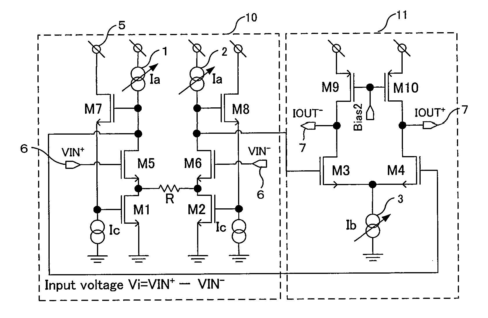
[0039]FIG. 1 shows a variable transconductance circuit of Embodiment 1. In a linear voltage current conversion section, which is configured as described in the prior art, an input voltage signal Vi is converted to a current with an inter-source resistance R between MOS transistors M5 and M6, to give a drain current for MOS transistors M1 and M2. At this time, the gate voltage difference between the MOS transistors M1 and M2 is represented by expression (4):

ΔVg=(Ia+ViRk1·β-Ia-ViRk1·β).(4)

where k1=gate width / gate length of MOS transistors M1 and M2 and β=charge mobility×capacity of gate oxide film / 2.

[0040]The gate voltages of the MOS transistors M1 and M2 are driven with the sources of MOS transistors M7 and M8 each constituting a source follower. If a substrate bias effect of the MOS transistors M7 and M8 is neglected, the above value ΔVg is equal to the gate voltage difference between the MOS transistors M7 and M8, that is, the drain voltage difference between the MOS transistors M5...

embodiment 2

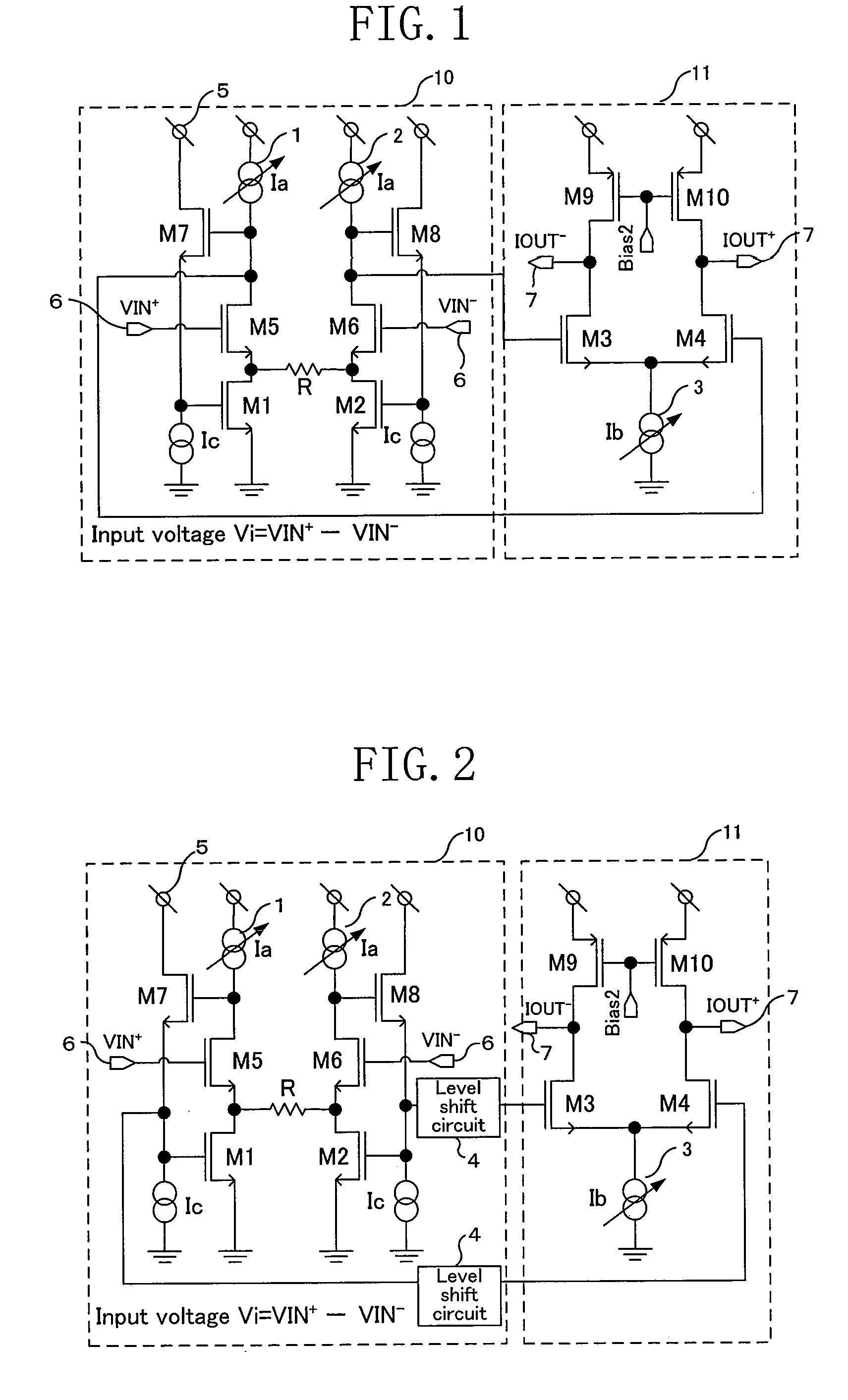
[0043]FIG. 2 shows a variable transconductance circuit of Embodiment 2. In the variable transconductance circuit of FIG. 1, the gate voltages of the MOS transistors M4 and M3 are automatically determined with the gate-source voltages of the MOS transistors M1 and M7 and the MOS transistors M2 and M8, respectively. Therefore, to allow operation of the MOS transistors M3 and M4 in the saturation region, the output dynamic range is automatically determined, and this restricts the degree of design freedom. To solve this problem, in the variable transconductance circuit of FIG. 2, a level shift circuit 4 is interposed each between the gates of the MOS transistors M1 and M4 and between the gates of the MOS transistors M2 and M3. By appropriately setting the DC level shift amount of each of the level shift circuits 4, the degree of design freedom of the output dynamic range is improved. Alternatively, if the input impedance is sufficiently high, the level shift circuit 4 may be interposed ...

embodiment 3

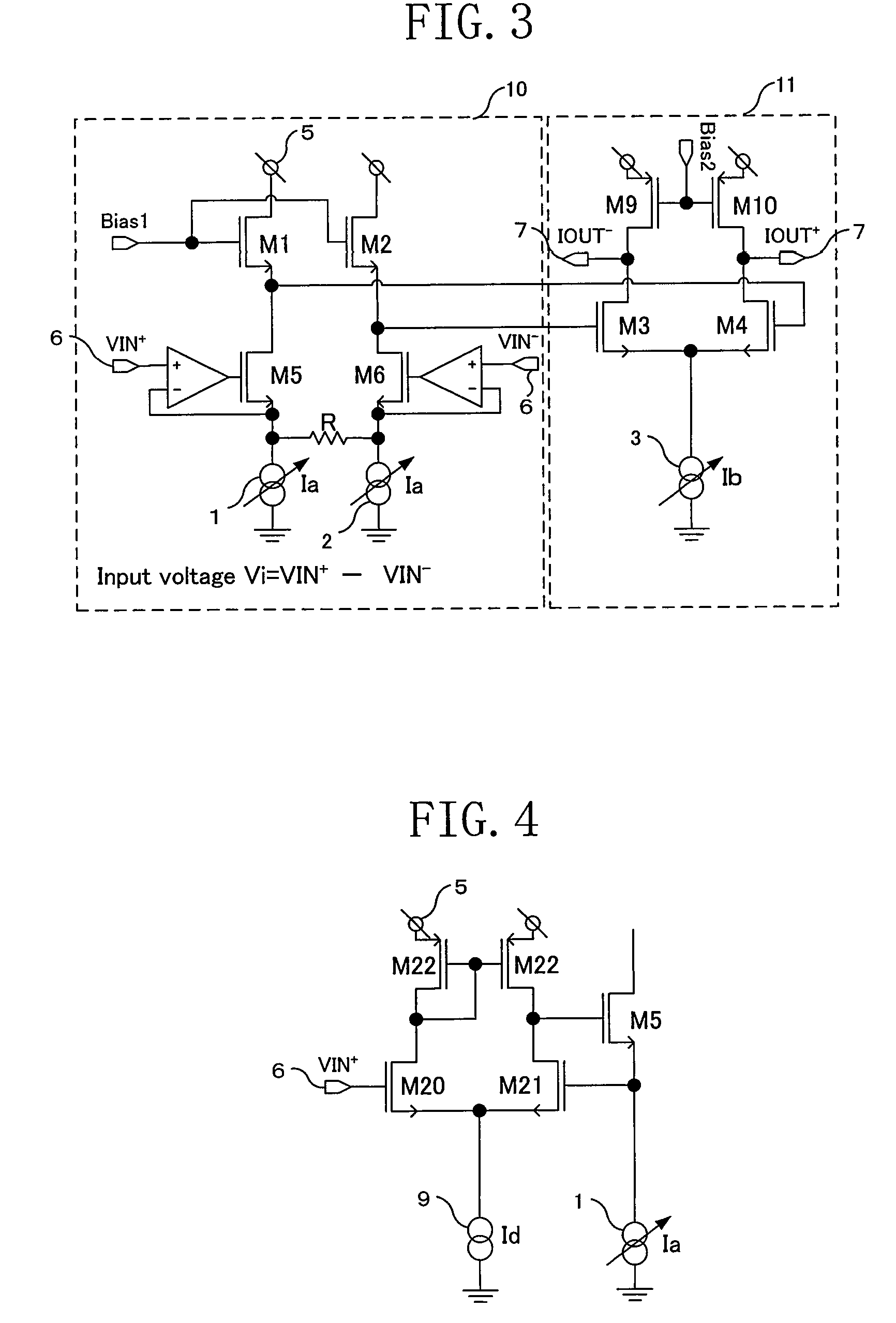
[0044]In the configurations in FIGS. 1 and 2, the MOS transistors M1, M5 and M7 or the MOS transistors M2, M6 and M8 constitute a negative feedback loop. The unity gain frequency f0 of such a loop and Ia have the relationship of Expression (8) below, and thus the circuit frequency characteristic varies with gm.

f0∝√{square root over (Ia)}   (8)

[0045]FIG. 3 shows a variable transconductance circuit of Embodiment 3 for solving the above problem. The MOS transistor M5 and a current source 1 constitute an output source follower for an operational amplifier, and the MOS transistor M6 and a current source 2 constitute another output source follower. The resistance R is connected between the outputs of the source followers. When the voltage signal Vi is input, the voltage difference of Vi also occurs at both ends of the resistance R, allowing flow of a signal current of Vi / R. This signal current, output from the drains of the MOS transistors M5 and M6, is input into the MOS transistors M1 a...


PUM


Abstract

The variable transconductance circuit includes: a voltage-current conversion circuit for outputting a current signal linear with an input voltage signal; first and second MOS transistors for converting the current signal received to a square-root compressed voltage signal; and third and fourth MOS transistors for converting the square-root compressed voltage signal to a linear current signal. A bias current at the first and second MOS transistors and a bias current at the third and fourth MOS transistors are varied to control transconductance.

Description

CROSS-REFERENCE TO RELATED APPLICATIONS[0001]This application claims priority under 35 U.S.C. § 119 on Patent Application No. 2005-198623 filed in Japan on Jul. 7, 2005 and Patent Application No. 2006-110550 filed in Japan on Apr. 13, 2006, the entire contents of which are hereby incorporated by reference.BACKGROUND OF THE INVENTION[0002]The present invention relates to a differential amplifier circuit, and more particularly, to a variable transconductance circuit formed on a semiconductor integrated circuit, and an optical disk device having such a variable transconductance circuit placed on a signal processing path.[0003]A conventional transconductance circuit disclosed in Japanese Laid-Open Patent Publication No. 11-68477 will be described with reference to FIG. 15.[0004]MOS transistors M50 and M51 constitute an input differential pair biased with a current Io. When a voltage signal Vi is input, MOS transistors M56 and M57 respectively drive gate voltages of MOS transistors M52 a...

Claims


Application Information

Patent Timeline
Patent Type & Authority Applications(United States)
IPC IPC(8): H03F3/45
CPCH03F3/45197H03F3/45201H03F2203/45288H03F2203/45356H03G7/001H03F2203/45652H03F2203/45668H03G1/0029H03F2203/45471
Inventor MORIKAWA, HIROYASUKATADA, MASAMICHINISHINAKA, MARIE
Owner PANASONIC SEMICON SOLUTIONS CO LTD
Why Eureka
Try Eureka