CMOS cross-coupled differential voltage controlled oscillator
- Summary
- Abstract
- Description
- Claims
- Application Information
AI Technical Summary
Benefits of technology
Problems solved by technology
Method used
Image
Examples
Embodiment Construction
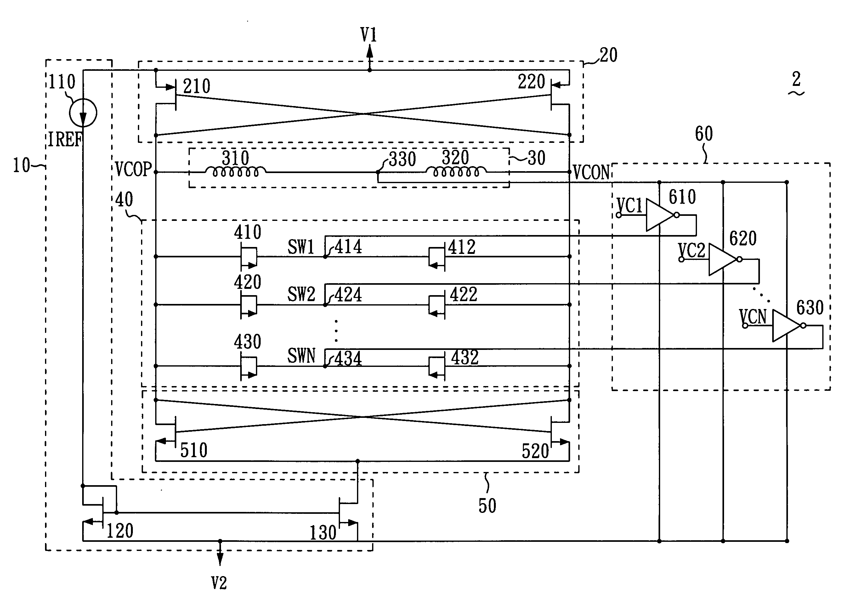
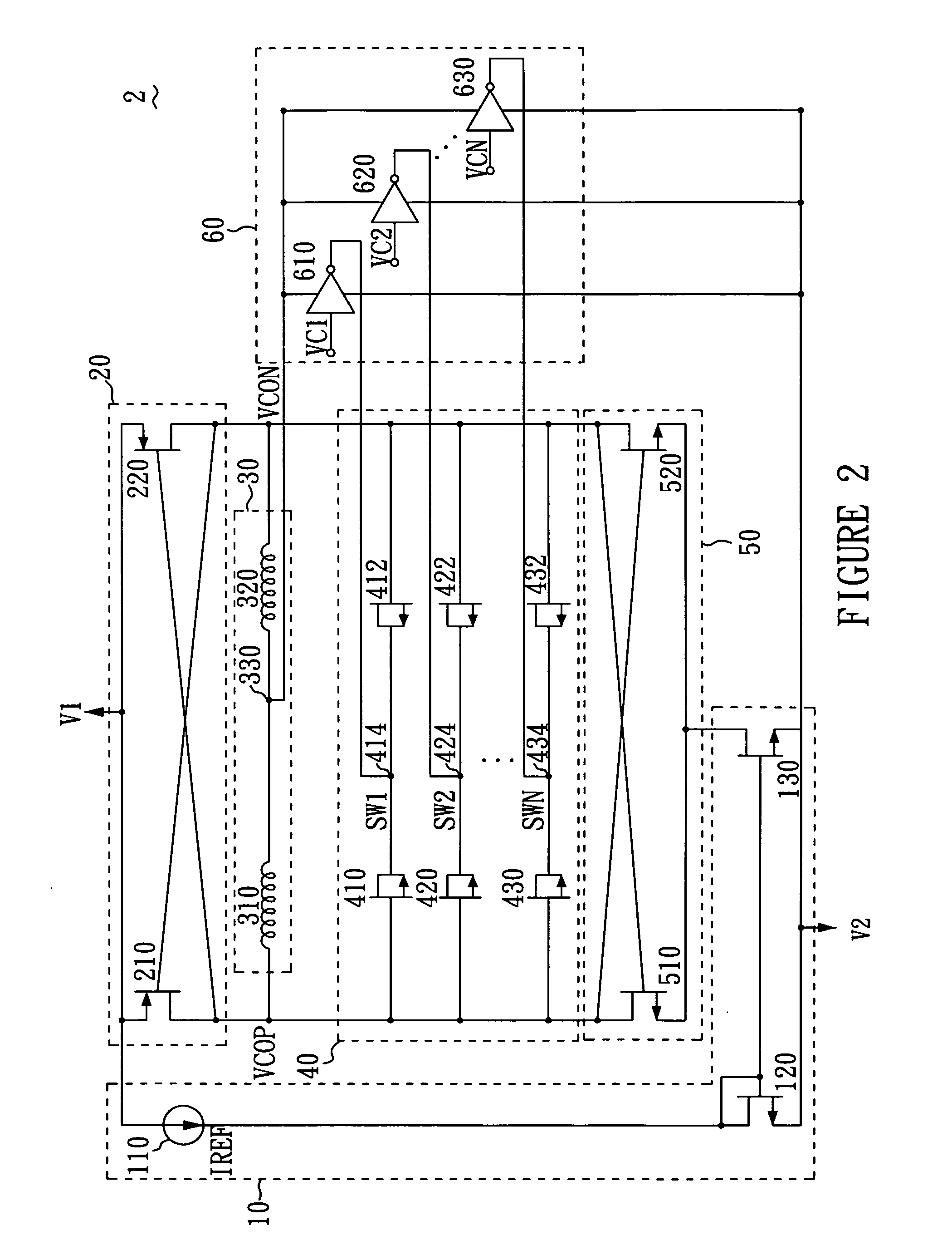
[0015]FIG. 2 shows a circuit diagram of a voltage controlled oscillator 2 of a preferred embodiment in accordance with the present invention. As shown in FIG. 2, the voltage controlled oscillator 2 includes power voltages V1 and V2, a current control unit 10, a first cross-coupled differential pair 20, an inductor unit 30, a capacitor unit 40, a second cross-coupled differential pair 50, voltage control unit 60, a plurality of voltage control signals VC1, VC2 . . . VCN and oscillator outputs VCON and VCOP. According to the present invention, the power voltage V1 is higher than the power voltage V2. The combinations of V1 and V2 can be VDD and GND, VDD and −VDD, or GND and −VDD, where GND refers to ground voltage, VDD can be 5V, 3.3V, 2.5V, 1.8V. The combinations applied here are used as examples demonstrating preferred embodiment and the scope of the present invention is not limited to above combinations.
[0016]The current control unit 10 comprises a current source 110, two NMOS fiel...
PUM
 Abstract
Description
Claims
Application Information


