Movable device

a technology of moving parts and components, applied in variable capacitors, generators/motors, instruments, etc., can solve the problems of low reliability, complicated structure, and troublesome production process

Inactive Publication Date: 2009-01-22
FUJITSU LTD
View PDF4 Cites 116 Cited by
  • Summary
  • Abstract
  • Description
  • Claims
  • Application Information

AI Technical Summary

Problems solved by technology

The result is a complicated structure where a large number of members are engaged with each other over four layers.
The production process also becomes troublesome.
On top of this, the torsion spring enabling tilt / return of the mirror 12 is made of metal which becomes fatigued and easily breaks upon repeated torsional deformation, so is low in reliability.
The conventional frequency bands are becoming overly congested.
With high frequency circuits or RF circuits, the interference between circuits (parasitic capacitance and parasitic resistance) has to be eliminated as much as possible, so current transistors which only switch between a low resistance state and high resistance state between ON / OFF are insufficient.
However, as such a switch, mounting together with an LSI enabling complicated circuits to be realized at a high density is demanded.
Up until now, there have been MEMS's mounted together with LSIs, but these have been large in size, low in operating speed, and large in power consumption, so complete integration with LSI's has not been achieved.
Competition arises for substrate space with the LSI circuits fabricated in the same monocrystalline substrate, so the degree of integration has been hard to improve.
Further, the process of production of MEMS's and the process of production of LSIs interfere with each other in temperature and formation of step differences, so the performances of the two deteriorate.
As a result, MEMS's produced at parts of semiconductor substrates have been exposed to the high temperature heat treatments required for LSI production and have unavoidably deteriorated in characteristics.
The precious library of LSI production technology built up through long experience cannot be effectively utilized and costs rise due to the expenses for development of new processes.
As explained above, conventional MEMS's are complicated in structure and cannot be reduced in size, so have the problems that they are slow in operating speeds, troublesome in production processes, and unavoidably high in costs and, further, are low in fatigue strength of the moving parts, so are low in reliability.
However, this only shows using a carbon nanotube to form a probe with a cantilever front end utilizing the microsize of the carbon nanotube.

Method used


Image

  • Movable device
  • Movable device
  • Movable device

Examples


embodiments

Embodiment 1

Reflection Mirror Device

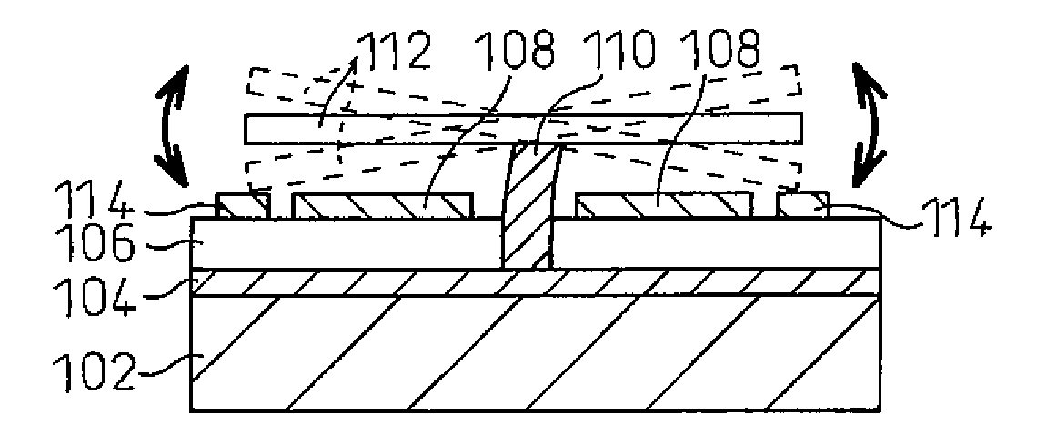
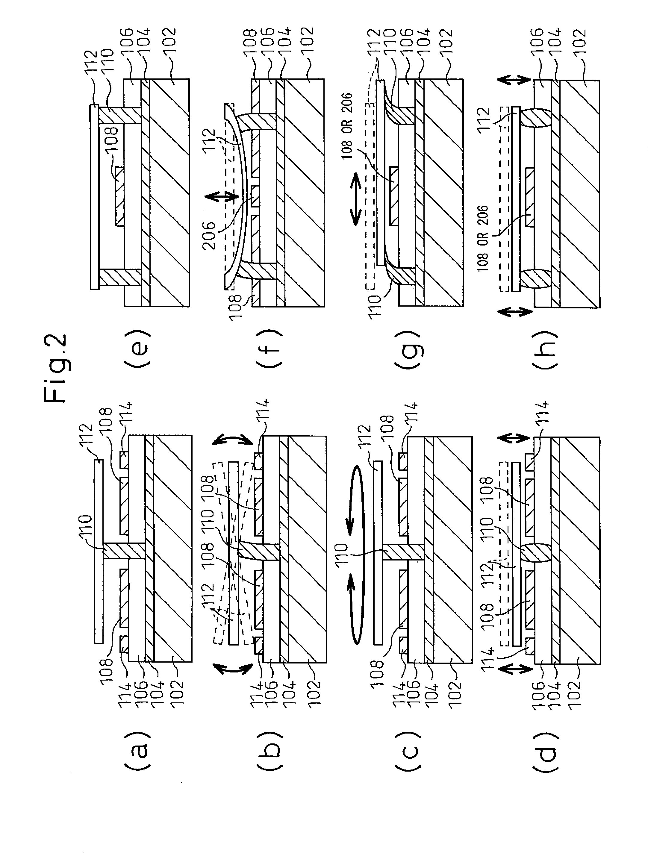
[0069]FIG. 4(1) is a longitudinal cross-sectional view of a reflection mirror device of an optical MEMS using a movable device of the present invention.

[0070]The illustrated reflection mirror device 100 is comprised of a substrate 102 on which a basic conductive layer 104, insulation layer 106, and a pair of left and right bottom electrodes 108L and 108R are formed in that order. A carbon nanotube elastic shaft 110 is fixed at its bottom end to the basic conductive layer 104 and passes upward through the insulation layer 106 to stand up. The top end of this elastic shaft 110 has the top electrode 112 fixed to it. The top surface of the top electrode 112 forms a mirror surface which functions as a reflection mirror. The insulation layer 106 has the function of reinforcing the joint between the bottom end of the carbon nanotube 110 and the basic conductive layer 104 so as to enable the superior mechanical properties of the carbon nanotube to be full...

embodiment 2

Multidirection Tilt

[0099]The reflection mirror device 100 of Embodiment 1 was shown in a mode tilting to the two directions of left and right, but the invention does not have to be limited to this. A mode tilting in larger directions is also possible.

[0100]For example, as shown in FIG. 8, the bottom electrodes 108 and stopper layers 114 are arranged radially in eight directions A to H centered about the carbon nanotube elastic shaft 110. By applying voltage between any one direction bottom electrode 108 among A to H and the top electrode 112, the top electrode 112 tilts in the direction of the bottom electrode 108 to which the voltage is applied. In this way, a reflection mirror device able to selectively tilt in eight directions can be realized.

embodiment 3

Multimirror

[0101]An example of a multimirror structure comprising reflection mirror devices 100 using the optical MEMS explained in Embodiment 1 arranged in a matrix will be explained.

[0102]The LSI device 126 shown in FIG. 9(1) is prepared by a multimirror structure shown in FIG. 9(2) using part of the connection pads 128 among a large number of connection pads 128, 130 as connection pads for optical communication. The other pads 130 are used for ordinary interconnect connections.

[0103]FIG. 9(2) is a plan view of a multimirror structure comprised of the MEMS reflection mirror devices 100 of Embodiment 1 arranged in a 5×5 matrix. The fine lines S show the outer edges of the regions occupied by the individual reflection mirror devices 100 and the boundary lines between adjoining mirror devices. If using reflection mirror devices 100 of the size of Embodiment 1, the areas of the pads 128 as a whole become 6.5×6.5 μm.

[0104]The optical communication pads 128 may be used for connecting a ...


PUM


Abstract

A movable device simultaneously enabling reduction of size down to the submicron level, higher speed operation, a streamlined production process, low costs, and greater reliability. A movable device provided with bottom electrodes and a basic conductive layer fixed to a substrate, an elastic shaft of a carbon nanotube with a bottom end fixed on the basic conductive layer and standing up, and a top structure including a top electrode spaced away from the bottom electrode and fixed to a top end of the elastic shaft, wherein when applying voltage between a bottom electrode and the top electrode, the top electrode displaces relatively to the bottom electrodes within an allowable range of elastic deformation of the elastic shaft.

Description

CROSS REFERENCE TO RELATED APPLICATIONS[0001]This application is a Continuation of International Application No. PCT / JP2006 / 306270, with an international filing date of Mar. 28, 2006, which designating the United States of America, the entire contents of which are incorporated herein by reference.TECHNICAL FIELD[0002]The present invention relates to a movable device simultaneously enabling reduction of the size, increase of the operating speed, streamlining of the production process, reduction of cost, and improvement of the reliability of an optical device etc. made by a conventional MEMS (Micro Electro Mechanical System).[0003]The movable device of the present invention can be applied advantageously as a movable device for an optical device (reflection mirror, light shutter, variable optical rotary device, variable condensing mirror), electrical switch (complete ON / OFF), memory (volatile, nonvolatile, multivalue), sensor (acceleration, angular acceleration, and mass), etc. (variab...

Claims


Application Information

Patent Timeline
Patent Type & Authority Applications(United States)
IPC IPC(8): H02N2/04G02B26/08G01P15/00
CPCB81B3/0059B81B2201/018B81B2201/047B81B2203/0109B81B2203/058B81B2203/053B81B2203/055B81B2203/056B81B2203/0181
Inventor NAKAMURA, SHUNJI
Owner FUJITSU LTD
Why Eureka
Try Eureka