Optical device, and production method for photonic crystal slab

Inactive Publication Date: 2009-01-22
PANASONIC CORP
View PDF7 Cites 5 Cited by
  • Summary
  • Abstract
  • Description
  • Claims
  • Application Information

AI Technical Summary

Benefits of technology

[0067]As is apparent from the description, the present invention has the effect of confining the

Problems solved by technology

For this reason, combinations of materials are limited.
However, an air bridge structure which uses the air as the cladding requires the photonic crystal to float in the air, and so its

Method used


Image

  • Optical device, and production method for photonic crystal slab
  • Optical device, and production method for photonic crystal slab
  • Optical device, and production method for photonic crystal slab

Examples


first embodiment

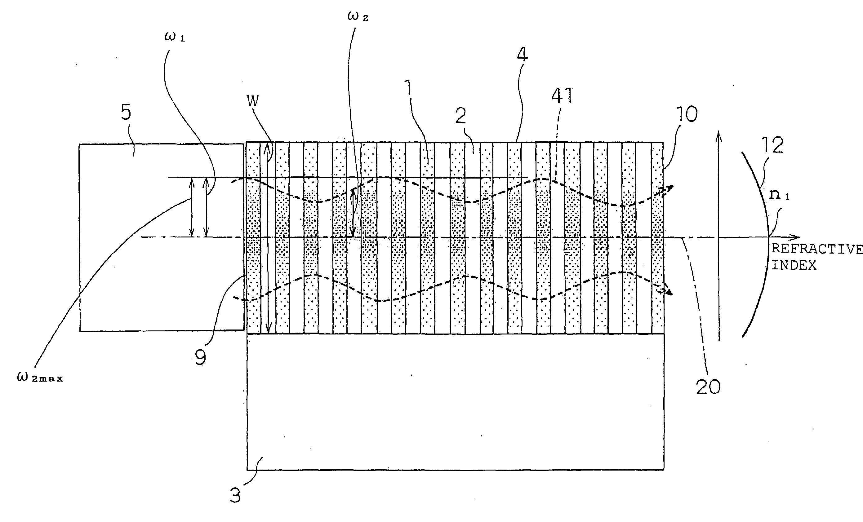
[0128]First, a principle of an optical device of the present invention will be described by mainly referring to FIGS. 1 and 2.

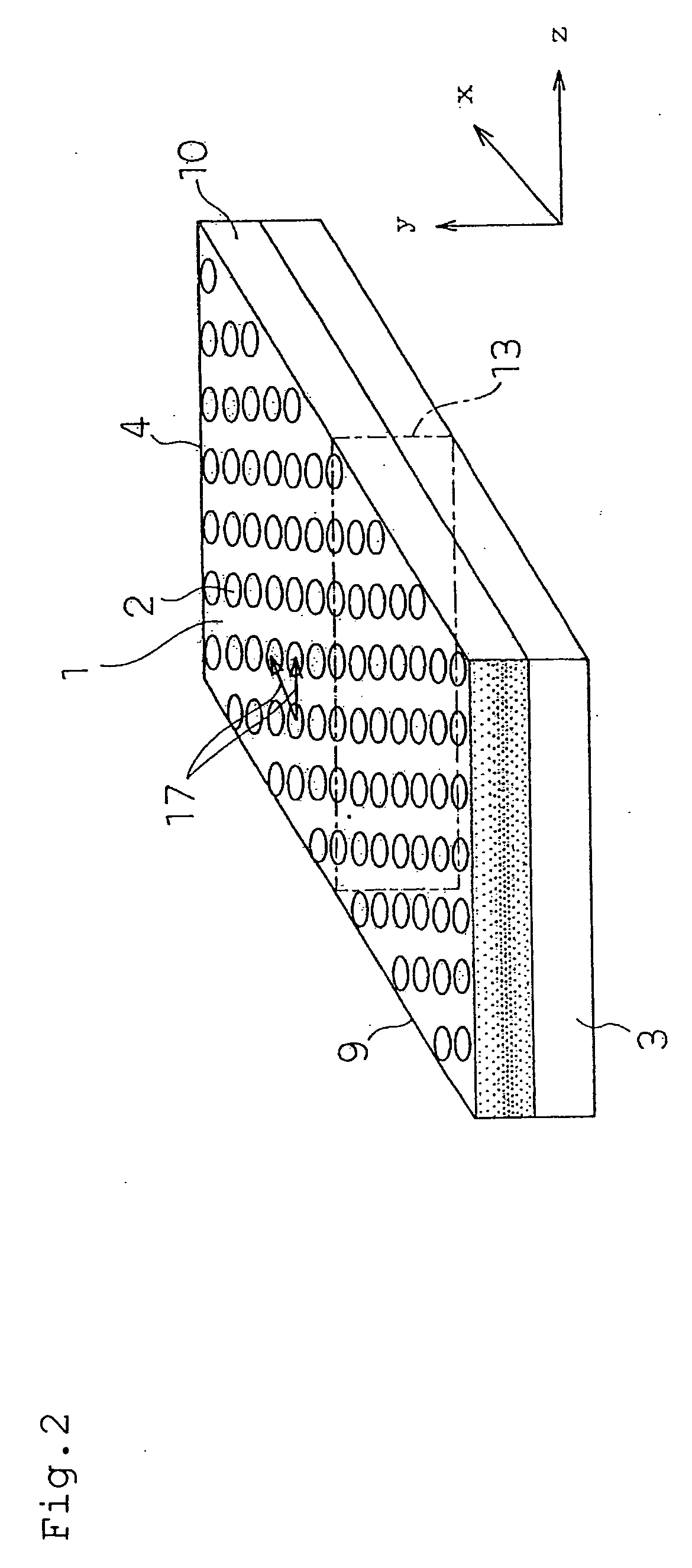
[0129]Here, FIG. 1 is a sectional view of a photonic crystal slab which has a refractive index distribution in which a refractive index becomes maximum around a center in a film thickness direction and lowers almost like a parabola as it becomes distant from the center (it is named a Graded-Index-type photonic crystal slab herein, and merely referred to as a GI-type photonic crystal slab hereafter). FIG. 1 is also a schematic view of a cross-section 13 (refer to FIG. 2) which includes the film thickness direction and a propagation direction. FIG. 2 is a perspective view of the GI-type photonic crystal slab which shows the position of the cross-section 13.

[0130]A beam spot trajectory 41 (refer to FIG. 1 and other drawings) changes discontinuously in a boundary portion between an incident side waveguide 5 (core refractive index: n0) and a GI-type photonic cryst...

second embodiment

[0197]Next, an embodiment of a manufacturing method of the photonic crystal slab of the present invention will be described by referring to FIGS. 16 (a) to 18.

[0198]FIGS. 16 (a) to 16 (d) are diagrams describing the characterizing portions of the manufacturing method as to the GI-type photonic crystal slab described in the first embodiment. To be more specific, these diagrams show a mechanism (which corresponds to a second process of the present invention), which forms the refractive index distribution in the film thickness direction on a sheet-like polysilane 1601 (which corresponds to the base material of a first process of the present invention) applied on the substrate 3 (refer to FIGS. 1 and 16 (d)) by means of heating and ultraviolet irradiation in the vertical direction.

[0199]First, the principle of the method which forms the refractive index distribution of the present invention will be described by referring to FIGS. 16 (a) to 16 (d).

[0200]As shown in FIG. 16 (a), the sheet...

third embodiment

[0218]Next, the configuration and operation of the optical device as an embodiment of the optical device of the present invention will be described by mainly referring to FIG. 9.

[0219]Here, FIG. 9 is a schematic sectional view which includes the film thickness direction and propagation direction of the GI-type photonic crystal slab which changes the refractive index distribution form according to partial change in the film thickness in order to satisfy the light confinement condition.

[0220]As shown in FIG. 9, the GI-type photonic crystal slab includes a reduced film thickness portion 90 wherein the film thickness W changes in a certain part of the z direction which corresponds to the propagation direction. And the refractive index distribution constant g is changed to a larger value against the film thickness changed to confine the light in the reduced film thickness portion 90 so as to satisfy the aforementioned light confinement condition (refer to FIG. 3).

[0221]As the film thickn...


PUM

PropertyMeasurementUnit
Thicknessaaaaaaaaaa
Radiusaaaaaaaaaa
Distributionaaaaaaaaaa

Abstract

An optical device which includes a GI-type photonic crystal slab which includes: a first member which has a distribution of refractive indexes reduced in both directions from an optical axis of incident light as to a first direction vertical to the optical axis; and a second member periodically placed in substance among the first members as to a second direction different from the first direction, wherein the distribution of refractive indexes of the first member which relates to the first direction, a thickness which relates to the first direction of the GI-type photonic crystal slab, a wavelength of the incident light and an incident end beam spot radius ω1 which relates to the first direction inside an incident end of the GI-type photonic crystal slab entered by the light of the incident light are determined to have the incident light substantially confined inside the GI-type photonic crystal slab as to the first direction.

Description

[0001]This application is a U.S. National Phase Application of PCT International Application PCT / JP2004 / 018509, filed Dec. 10, 2004.TECHNICAL FIELD[0002]The present invention relates to an optical device which uses a photonic crystal slab used for a filter, a prism, a waveguide, an optical plane circuit and the like and a manufacturing method of the photonic crystal slab.BACKGROUND ART[0003]A conventional photonic crystal slab is configured by a two-dimensional photonic crystal which has multiple columnar portions (refractive index=v1) arranged in a two-dimensional cycle in a slab of a fixed refractive index (refractive index=v2), a lower cladding and an upper cladding (refractive index=v3) of a lower refractive index than v1, v2, which sandwich the two-dimensional photonic crystal in a film thickness direction and a substrate.[0004](1) Light propagating in the photonic crystal slab is confined in a vertical direction by total reflection at a boundary with the upper and lower claddi...

Claims


Application Information

Patent Timeline
IPC IPC(8): G02B6/10C03B37/022G02B1/02G02B6/12G02B6/122
CPCG02B6/1225B82Y20/00
Inventor HAMADA, HIDENOBU
Owner PANASONIC CORP
Why Eureka
Try Eureka