Tunnel Junction Barrier Layer Comprising a Diluted Semiconductor with Spin Sensitivity

a tunnel junction and barrier layer technology, applied in the direction of substrate/intermediate layer, magnetic body, instruments, etc., can solve the problems of mr typically degraded, source of noise, and extremely difficult to realize true half metals in practice, and achieve enhanced mr effect, low barrier height, and tunable resistance

Inactive Publication Date: 2009-02-12
SPINTRONIX AB
View PDF2 Cites 3 Cited by
  • Summary
  • Abstract
  • Description
  • Claims
  • Application Information

AI Technical Summary

Benefits of technology

[0008]The invention is a magnetic tunnel junction in which the prior art alumina tunneling barrier layer is replaced by a tunneling barrier layer consisting of a ferromagnetic semiconductor with lower barrier height and with a spin filter function. Since spin sensitivity thereby is introduced in the barrier layer, this allows a replacement of one of the ferromagnetic electrodes of prior art to a non-magnetic electrode. A MTJ device comprising such a spin filter barrier with a low effective barrier height promises enhancement of the MR effect with tunable resistance and a simpler MTJ device structure. Even though the invention has been summarized above, the invention is defined by the enclosed claims 1-10.

Problems solved by technology

For example, alternative electrode materials such as the so-called half-metallic ferro magnets with predicted spin-polarization of close to 100% [3] have been attempted but true half metals have been proven to be extremely difficult to realize in practice [4].
Therefore, the barrier layer resistance is also the main source of noise in a MTJ device.
At this thickness regime the MR is typically degraded, most likely due to the formation of quantum point defects and / or microscopic pin holes in the ultra thin tunnel barrier layer needed to obtain these very low RA values.

Method used


Image

  • Tunnel Junction Barrier Layer Comprising a Diluted Semiconductor with Spin Sensitivity
  • Tunnel Junction Barrier Layer Comprising a Diluted Semiconductor with Spin Sensitivity
  • Tunnel Junction Barrier Layer Comprising a Diluted Semiconductor with Spin Sensitivity

Examples


Embodiment Construction

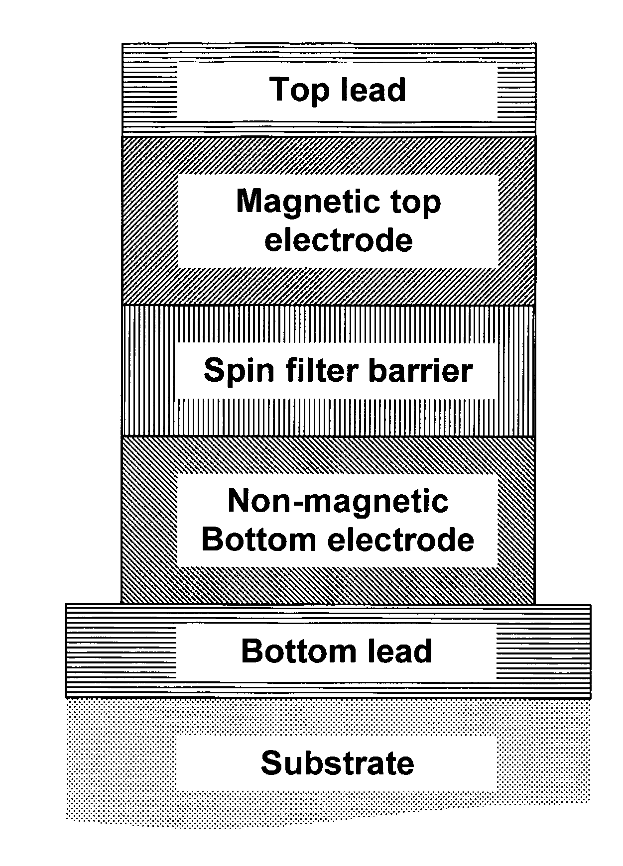
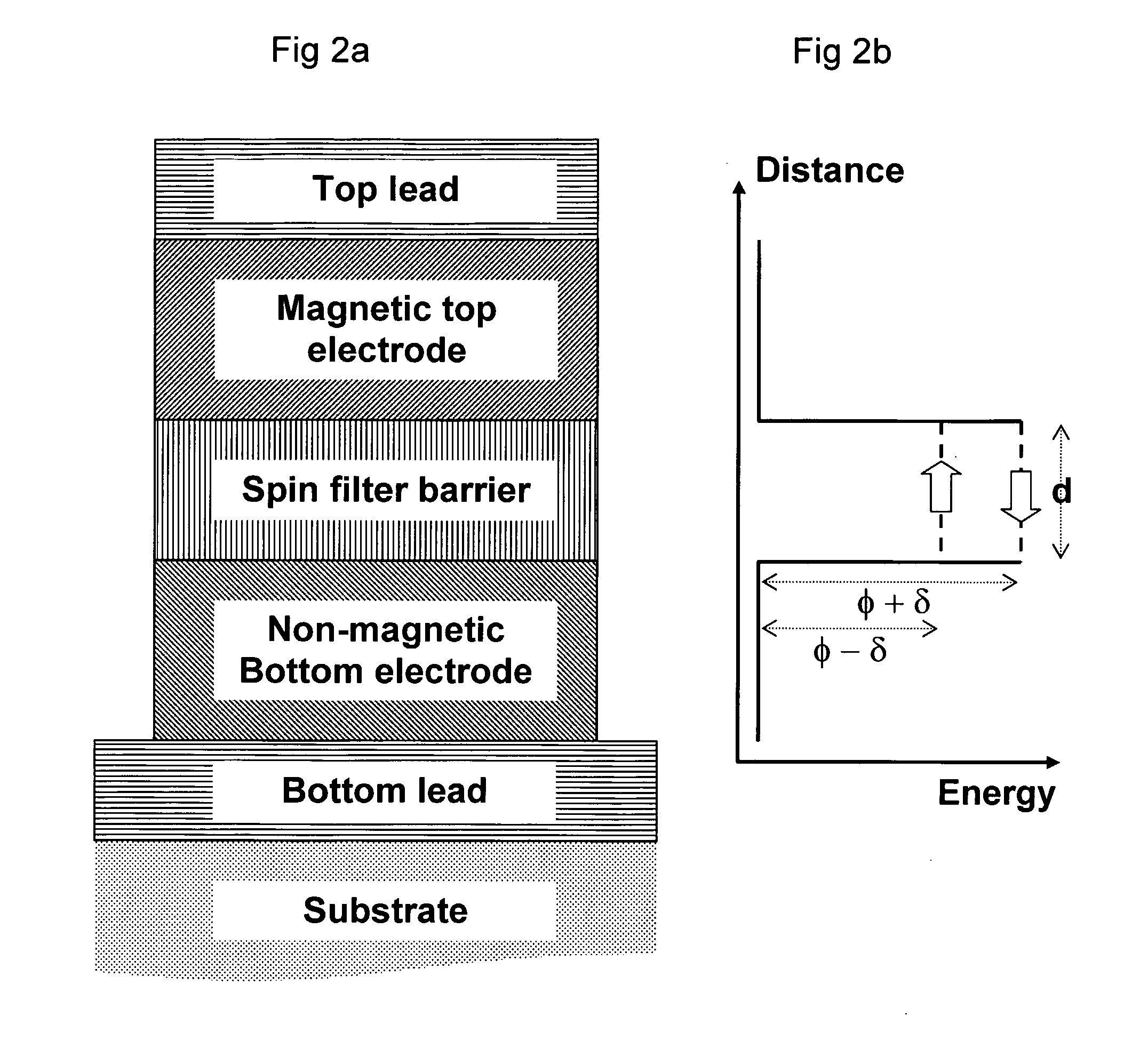
[0016]Conventional MTJ devices offer little room for further improvements due to the restricted spin-polarization of the electrodes and the high RA of the alumina barrier. In particular, much effort has been put down to develop efficient methods to reduce the alumina barrier thickness to the ultra-thin regime with preserved barrier uniformity. This has shown to be extremely difficult. The present invention comprises an alternative type of MTJ device structure that has the potential to provide a higher spin-polarization at reduced RA values compared to the conventional MTJ device

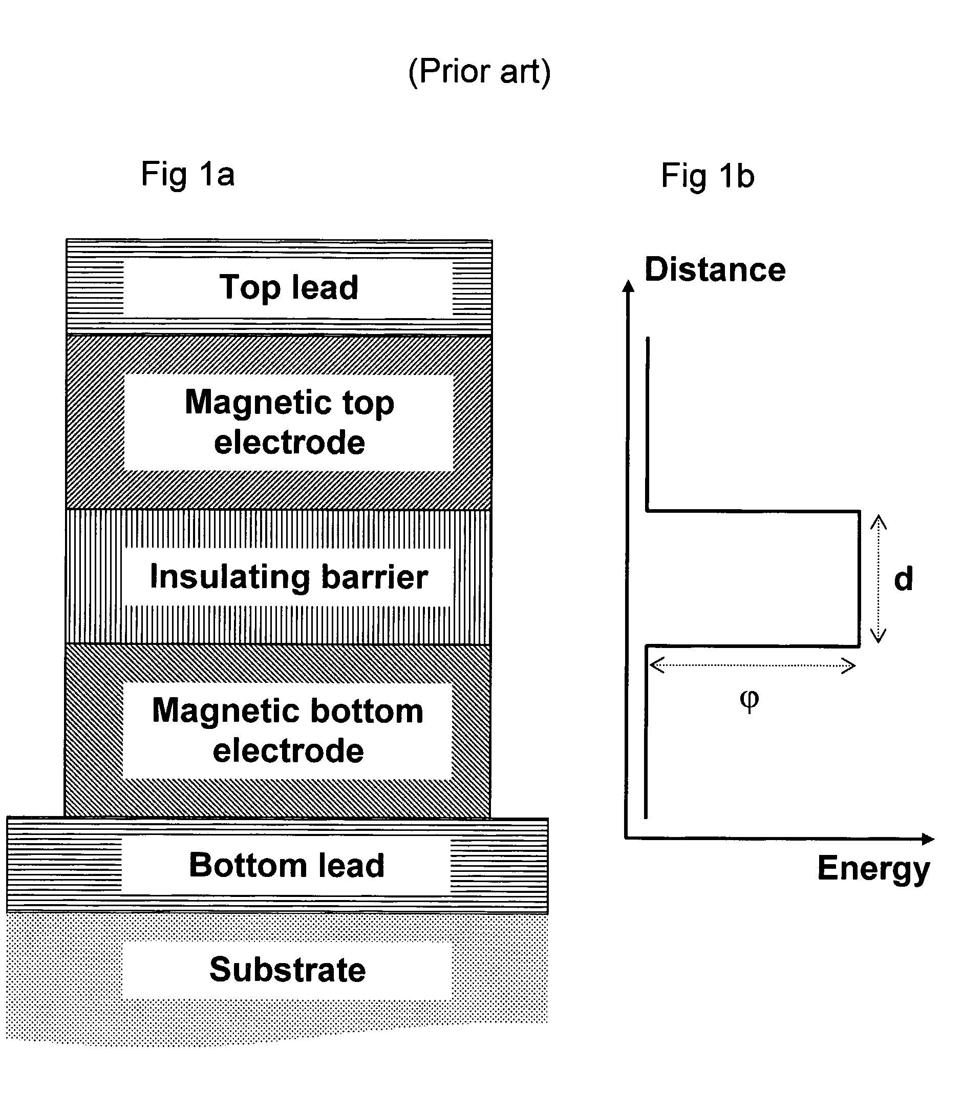
[0017]FIG. 1 (a) shows the cross-sectional MTJ device structure of prior art. The bottom ferromagnetic electrode layer (“fixed” layer), in most cases Co, is usually grown onto an antiferromagnetic layer (not shown) such as CoO that via exchange bias establishes a permanent magnetization direction of the bottom ferromagnetic electrode. The purpose of this is to make the bottom electrode insensitive to external...


PUM

PropertyMeasurementUnit
magneticaaaaaaaaaa
Magnetic Resistanceaaaaaaaaaa
magneto resistanceaaaaaaaaaa

Abstract

The invention provides a magnetic tunnel junction having a tunneling barrier layer wherein said tunneling barrier layer comprises a diluted magnetic semiconductor with spin sensitivity. The magnetic tunnel junction may according to the invention comprise a bottom lead coupled to a bottom electrode which is coupled to a diluted magnetic semiconductor coupled to a top electrode being coupled to a top lead, wherein said bottom electrode is non magnetic. The invention further provides various components and a computer, exploiting the magnetic tunnel junction according to the invention.

Description

TECHNICAL FIELD OF THE INVENTION[0001]The invention relates to Magnetic Tunnel Junction (MTJ) devices for spin-sensitive electronic and optical applications. These applications include non-volatile magnetic random access memories (MRAMs), magneto resistive read heads for magnetic disk drives, spin-valve / magnetic-tunnel transistors, ultra-fast optical switches and light emitters with polarization modulated output. Other applications, within which the invention can be incorporated as a sub-system, are logic devices with variable logic function and quantum computers. In particular, the invention uses a tunnel barrier with a spin-filter function to improve the properties and performance of MTJs.BACKGROUND OF THE INVENTION[0002]Magnetic Tunnel Junctions (MTJs) are devices that exploit the magneto resistance effect to modulate electrical conductivity. A MTJ device comprises two ferromagnetic electrodes separated by an insulating barrier layer made sufficiently thin to allow quantum-mechan...

Claims


Application Information

Patent Timeline
Patent Type & Authority Applications(United States)
IPC IPC(8): H01L29/43G11CG11C11/16H01F1/40H01F10/193H01F10/32H01L29/66H01L43/08
CPCB82Y25/00G11C11/16H01F1/402H01F41/325H01F10/3254H01L43/08H01L43/10H01F10/193H10N50/10H10N50/85H10N50/00H01F1/401H01L29/66984
Inventor GUSTAVSSON, FREDRIK
Owner SPINTRONIX AB
Why Eureka
Try Eureka