Method of manufacturing nanoelectrode lines using nanoimprint lithography process

a nano-imprint lithography and nano-electrode technology, applied in photomechanical treatment, instruments, electrical equipment, etc., can solve the problems of mold and substrate deformation or damage, difficult to form superfine patterns, and long formation time of large patterns

Inactive Publication Date: 2009-01-22
ELECTRONICS & TELECOMM RES INST
View PDF6 Cites 28 Cited by
  • Summary
  • Abstract
  • Description
  • Claims
  • Application Information

AI Technical Summary

Problems solved by technology

However, since a circuit linewidth or a pattern linewidth is determined by the wavelength of light used for the exposure process, it is not easy to form superfine patterns, for example, 100 nm fine patterns, on the substrate using the photolithography process.
However, since the nanoimprint lithography process is performed under a high process pressure, the mold and the substrate may be deformed or damaged.
Also, the polymer thin layer can be patterned using the flowability of a heated polymer material, so that formation of large patterns takes much time.
When nanoelectrode lines are manufactured using the conventional imprint lithography process as described above, the foregoing drawbacks may lead to interaction (e.g., electrical connection) between the metal electrode lines, thus making it difficult to form independent metal electrodes.
However, according to these conventional methods, it is still difficult to form completely independent metal electrode lines to sub-micrometer levels.

Method used


Image

  • Method of manufacturing nanoelectrode lines using nanoimprint lithography process
  • Method of manufacturing nanoelectrode lines using nanoimprint lithography process
  • Method of manufacturing nanoelectrode lines using nanoimprint lithography process

Examples


Embodiment Construction

[0018]The present invention will now be described more fully with reference to the accompanying drawings, in which exemplary embodiments of the invention are shown. This invention may, however, be embodied in different forms and should not be construed as limited to the embodiments set forth herein.

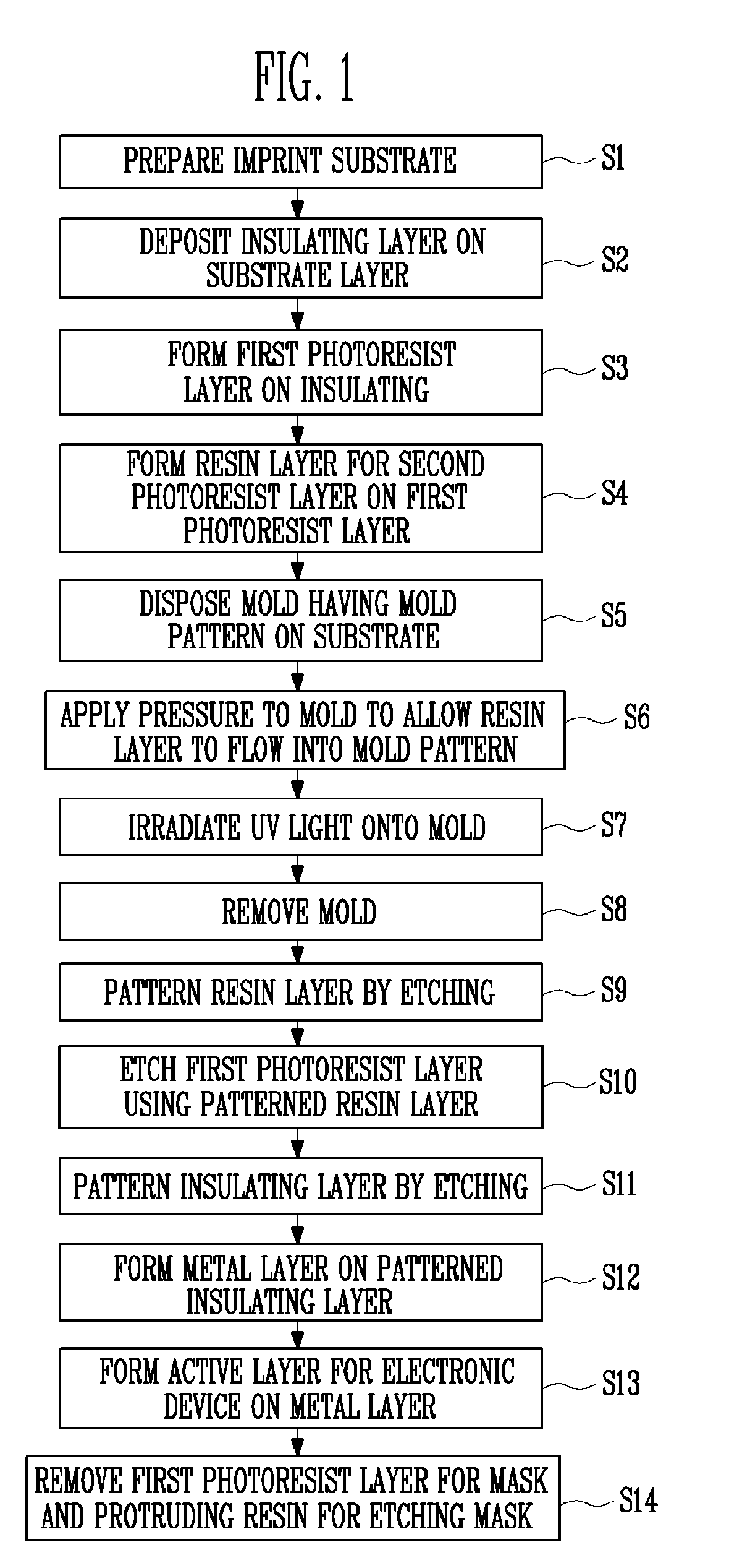
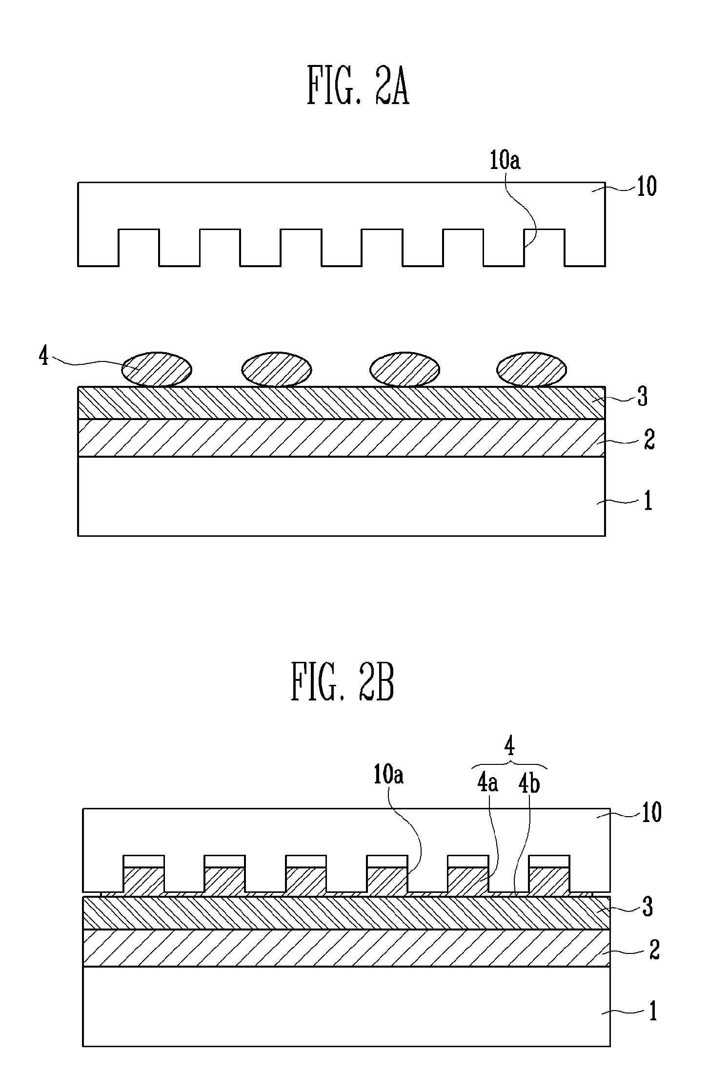
[0019]FIG. 1 is a flowchart illustrating a method of manufacturing nanoelectrode lines between insulating layer patterns using a nanoimprint lithography process according to an exemplary embodiment of the present invention, and FIGS. 2A through 2J are cross-sectional views illustrating the method shown in FIG. 1.

[0020]Referring to FIGS. 1 and 2A, first, an imprint substrate 1 is prepared in step S1. The imprint substrate 1 may be a silicon wafer. In the present embodiment, the silicon wafer may be a 200-mm thick double-sided silicon wafer.

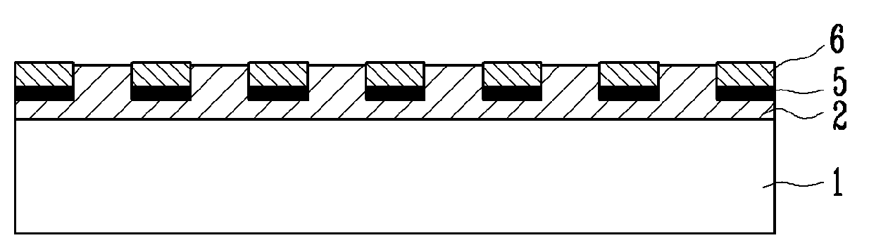
[0021]In step S2, an insulating layer 2 is deposited on the imprint substrate 1. The insulating layer 2 is formed of one of SiO2, SiNx, and alumina to a...


PUM

PropertyMeasurementUnit
wavelengthaaaaaaaaaa
thicknessaaaaaaaaaa
temperatureaaaaaaaaaa

Abstract

Provided are a method of manufacturing nanoelectrode lines. The method includes the steps of: sequentially forming an insulating layer, a first photoresist layer, and a drop-shaped second photoresist on a substrate; disposing an imprint mold having a plurality of molding patterns over the second photoresist; applying pressure to the mold to allow the second photoresist to flow into the mold patterns; irradiating ultraviolet (UV) light onto the mold to cure the second photoresist; removing the mold from the cured second photoresist and patterning the second photoresist; patterning the first photoresist layer using the patterned second photoresist as a mask; patterning the insulating layer; and forming a metal layer between the patterned insulating layers. In this method, metal electrode lines are formed between insulating layers using an imprint lithography process, so that nanoelectronic devices can be freed from crosstalk between the metal electrode lines.

Description

CROSS-REFERENCE TO RELATED APPLICATION[0001]This application claims priority to and the benefit of Korean Patent Application No. 2007-71993, filed Jul. 19, 2007, the disclosure of which is incorporated herein by reference in its entirety.BACKGROUND[0002]1. Field of the Invention[0003]The present invention relates to a method of manufacturing nanoelectrode lines for nanoelectronic devices and, more particularly, to a method of manufacturing nanoelectrode lines between insulating layer patterns using a nanoimprint lithography process.[0004]2. Discussion of Related Art[0005]Conventionally, manufacture of semiconductor devices, electronic devices, photoelectric devices, magnetic devices, and display devices involves a photolithography process of forming fine patterns on a substrate. The photolithography process includes coating a substrate including a polymer layer with a polymer material having reactivity to light, exposing the polymer material to light by allowing light to pass throug...

Claims


Application Information

Patent Timeline
Patent Type & Authority Applications(United States)
IPC IPC(8): H01L21/768
CPCB82Y10/00B82Y40/00H01L51/0022H01L21/0331H01L21/31144G03F7/0002Y10S977/889H10K71/611H01L21/0272
Inventor JEONG, MI HEELEE, HYO YOUNGCHOI, NAK JINPARK, KANG HO
Owner ELECTRONICS & TELECOMM RES INST
Why Eureka
Try Eureka