Light emitting device and method of manufacturing the same

a technology lead electrodes, which is applied in the direction of semiconductor devices, semiconductor/solid-state device details, electrical apparatus, etc., can solve the problems of insufficient bonding strength, low bonding between light emitting elements and lead electrodes, and the expected improvement of light extracting efficiency of light emitting devices

Active Publication Date: 2009-01-29
NICHIA CORP
View PDF2 Cites 45 Cited by
  • Summary
  • Abstract
  • Description
  • Claims
  • Application Information

AI Technical Summary

Problems solved by technology

However, bonding between the light emitting element and the lead electrode is low and sufficient bonding strength cannot be obtained.
In a case where a light emit...

Method used


Image

  • Light emitting device and method of manufacturing the same
  • Light emitting device and method of manufacturing the same
  • Light emitting device and method of manufacturing the same

Examples


embodiment 1

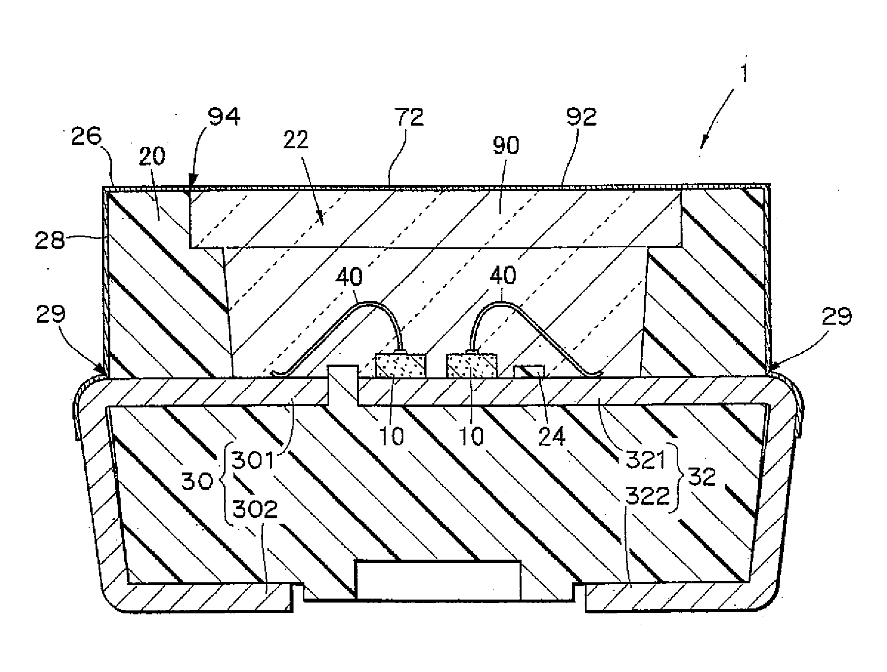
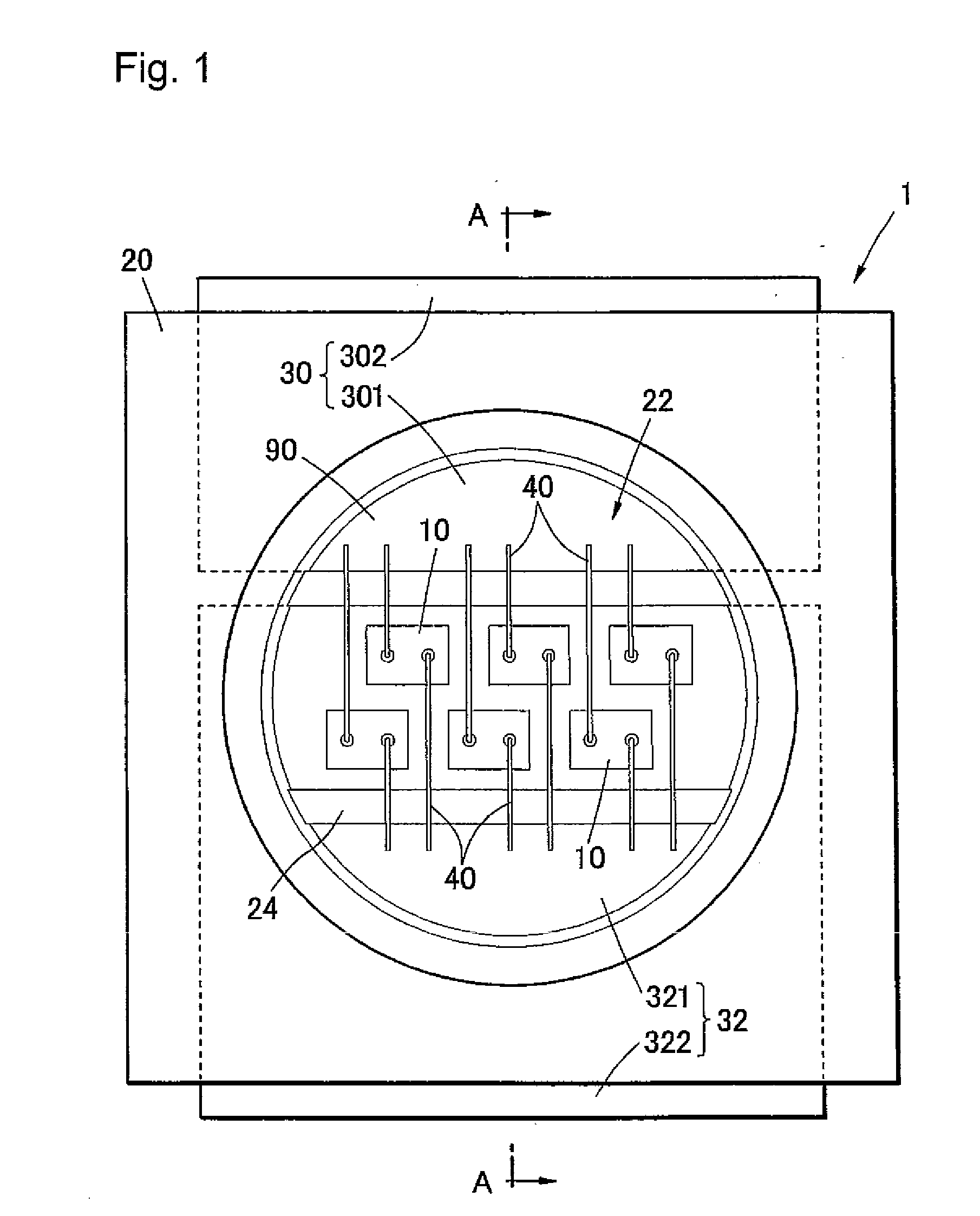
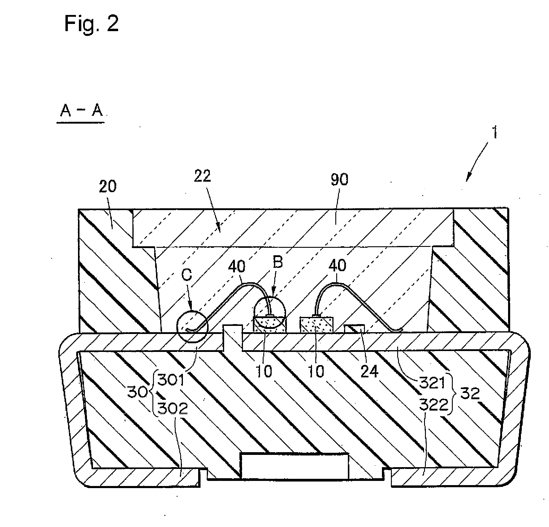
[0033]FIG. 1 and FIG. 2 show a light emitting device 1 according to the present embodiment, provided with a package using a lead frame as a base. Light emitting elements 10 are mounted face-up within a recess 22 of a package 20. Further, a pair of lead electrodes (first electrode 30, second electrode 32) are placed penetrating the package 20 as electrically conductive members. An end portion of each lead electrode 30, 32 is exposed in the recess 22 to form an inner conductive portion (lead electrode) 301, 321, respectively. The other end of each lead electrode 30, 32 penetrates through the package 20 to form an external conductive portion (external terminal) 302, 322, respectively. A pair of electrodes (not shown) disposed on each of the light emitting elements 10 are electrically connected to a pair of lead terminals (first lead terminal 301, second lead terminal 322) via conductive wires 40 respectively.

[0034]FIG. 3 is a partially enlarged cross sectional view of a bonding portion...

embodiment 2

[0083]The light emitting device 1 shown in FIG. 13 is of a type which includes a package that has a lead frame as its base, as in Embodiment 1. Arrangement of the light emitting elements 10, wiring of the conductive wires 40, and shapes of the first lead electrodes 30 and the second lead electrode 32 are different from that in Embodiment 1. Further, in the present embodiment, a mounting portion 36 which is different from the lead electrode is provided to mount the light emitting elements 10.

[0084]In the present embodiment, as shown in FIG. 13, adjacent light emitting elements 10 are connected with the conductive wires 40 so that a plurality of the light emitting elements 10 are electrically connected in series. In this wiring, the conductive wire 40 is thermally compressed to each of the light emitting elements 10 between the first bond 50 and the second bond 60. In the present specification, such a thermally compressed portion is referred to as “stitch bond 68” and the wiring type ...

examples

[0088]A plurality of samples with modified structures are formed according to the light emitting device 1 shown in FIG. 1 and FIG. 13, and a lighting test is performed.

(1. Formation of Package 20)

[0089]As measurement samples, packages of a lead frame type and a substrate type are formed. In case of packages of lead frame type, a lead frame made of a copper-alloy is used, and in case of the samples indicated as Ag in “Covering material of lead frame”, Ag film is disposed on the surface of the lead frame. A thermoplastic resin (polyphthalamide) is used for the package material and the packages are made by injection molding.

[0090]In case of packages of substrate type, a ceramics substrate of Al2O3 or a glass epoxy substrate provided with electrode wiring is used.

(2. Die Bonding Step)

[0091]A light emitting element 10 is die-bonded onto each package by way of resin bonding using a silicone resin binding material, a modified silicone binding material, an epoxy resin bonding material, or t...


PUM


Abstract

Provided is a light emitting device with high extraction efficiency, in which absorption of light by a conductive wire is prevented effectively. The light emitting device includes a conductive wire electrically connecting an electrode of a light emitting element and an electrically conductive member. The surface of the bonding portion of the conductive wire between the conductive wire and at least one of the electrode of the light emitting element and the electrically conductive member is covered with a metal film. The reflectivity of the metal film is higher than that of the conductive wire at the emission peak wavelength of the light emitting element.

Description

BACKGROUND OF THE INVENTION[0001]1. Technical Field[0002]The present invention relates to a light emitting device including a light emitting element, and more particularly, to a light emitting device having high light extraction efficiency of light emitted from the light emitting element.[0003]2. Background Art[0004]Among ways to improve the light extraction efficiency of a light emitting device, enhancement of the reflectance in a package where a light emitting element to be mounted has been actively conducted. Provision of a metal film on the light incident surface receiving light from the light emitting element is one of the known methods to enhance the reflectivity, as disclosed in JP2006-324438A for example. In the light emitting device disclosed in JP2006-324439A, silver plating is applied on the mounting surface, which is a heat sink, so as to use the mounting surface as a light reflecting member, thus improves the light extraction efficiency of the light from the light emitt...

Claims


Application Information

Patent Timeline
IPC IPC(8): H01L33/00H01L21/00H01L33/46H01L33/62
CPCH01L24/45H01L2924/12041H01L25/0753H01L33/46H01L33/62H01L2224/45124H01L2224/45139H01L2224/45144H01L2224/45147H01L2224/4516H01L2224/45184H01L2224/48091H01L2224/48137H01L2224/48247H01L2224/48465H01L2224/48599H01L2224/48699H01L2224/8592H01L2224/97H01L2924/01012H01L2924/01013H01L2924/01014H01L2924/01015H01L2924/01029H01L2924/0103H01L2924/01032H01L2924/01046H01L2924/01047H01L2924/0105H01L2924/01078H01L2924/01079H01L2924/01082H01L2924/014H01L2924/09701H01L2924/16195H01L24/48H01L2224/49175H01L24/97H01L2924/10329H01L2924/01074H01L2924/01033H01L2924/01005H01L2924/01006H01L2924/01019H01L2924/01023H01L2224/85H01L2924/00014H01L2924/00012H01L2924/00H01L2224/45015H01L2924/15787H01L2924/12035H01L2924/12036H01L2924/181H01L2224/49113H01L24/49H01L2224/48139H01L2924/20752H01L2924/00015
Inventor HAYASHI, MASAKIOKADA, YUJIKURODA, KOJI
Owner NICHIA CORP
Why Eureka
Try Eureka