Liquid crystal display device and method of manufacturing the liquid crystal display device

a liquid crystal display and liquid crystal technology, applied in semiconductor devices, instruments, optics, etc., can solve the problems of residual deposits peeling or poor connection of the upper layer electrode due to residual deposits, and the contact resistance may increas

Active Publication Date: 2009-01-29
JAPAN DISPLAY WEST
View PDF9 Cites 32 Cited by
  • Summary
  • Abstract
  • Description
  • Claims
  • Application Information

AI Technical Summary

Benefits of technology

[0015]In addition, further another aspect of the invention provides a liquid crystal display device. The liquid crystal display device includes a switching element, a common electrode line, a first insulating film, a first etching stopper electrode, a pixel electrode, a second insulating film and a common electrode. The switching element has a drain electrode and is arranged on a substrate. The common electrode line is arranged on the substrate. The first insulating film covers the switching element, the drain electrode and the common electrode line, and has a first opening on the drain electrode and a second opening on the common electrode line. The first etching stopper electrode is formed in the second opening and is connected to the common electrode line. The pixel electrode is arranged on the first insulating film. The second insulating film covers the first etching stopper electrode and the pixel electrode, and has a third opening on the first etching stopper electrode. The common electrode is connected through the third opening to the first etching stopper electrode and extends onto the second insulating film so as to face the pixel electrode. In addition, the liquid crystal display device of the aspect of the invention may further include a lower layer electrode for external connection, a second etching stopper electrode, and an upper layer electrode for external connection, wherein the lower layer electrode is arranged on the substrate and is covered with the first insulating film, wherein the second etching stopper electrode is formed on the first insulating film and is connected through an opening of the first insulating film to the lower layer electrode, and wherein the upper layer electrode is formed on the second insulating film and is connected to the second etching stopper electrode in an opening of the second insulating film. In addition, the liquid crystal display device according to the aspect of the invention may further include an opposite substrate that is arranged so as to face the substrate and a liquid crystal that is held between the substrate and the opposite substrate, wherein an alignment direction of the liquid crystal is controlled by an electric field generated between the common electrode and the pixel electrode.

Problems solved by technology

However, according to a method of manufacturing the above liquid crystal display device, in a process in which the drain electrode of the pixel transistor is connected to the pixel electrode, there has been a possibility that a contact resistance may increase because a residual deposit produced during dry etching intervenes between these electrodes.
In addition, a residual deposit also intervenes between the lower layer electrode and upper layer electrode of the terminal portion, so that there has been a possibility that not only an increase in contact resistance but also peeling or poor connection of the upper layer electrode due to the residual deposit may occur.
As a result, there has been a problem, such as poor display or delay of signal transmission.
Thus, poor formation occurs and, hence, reduces yields.

Method used


Image

  • Liquid crystal display device and method of manufacturing the liquid crystal display device
  • Liquid crystal display device and method of manufacturing the liquid crystal display device
  • Liquid crystal display device and method of manufacturing the liquid crystal display device

Examples


Embodiment Construction

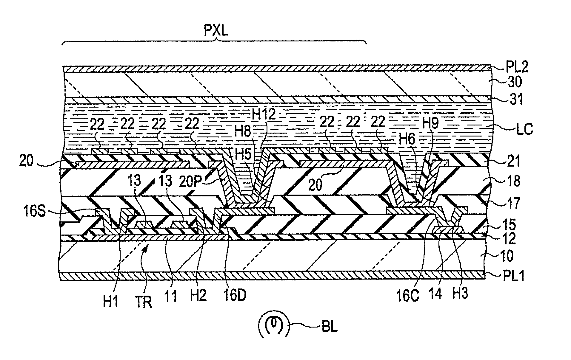
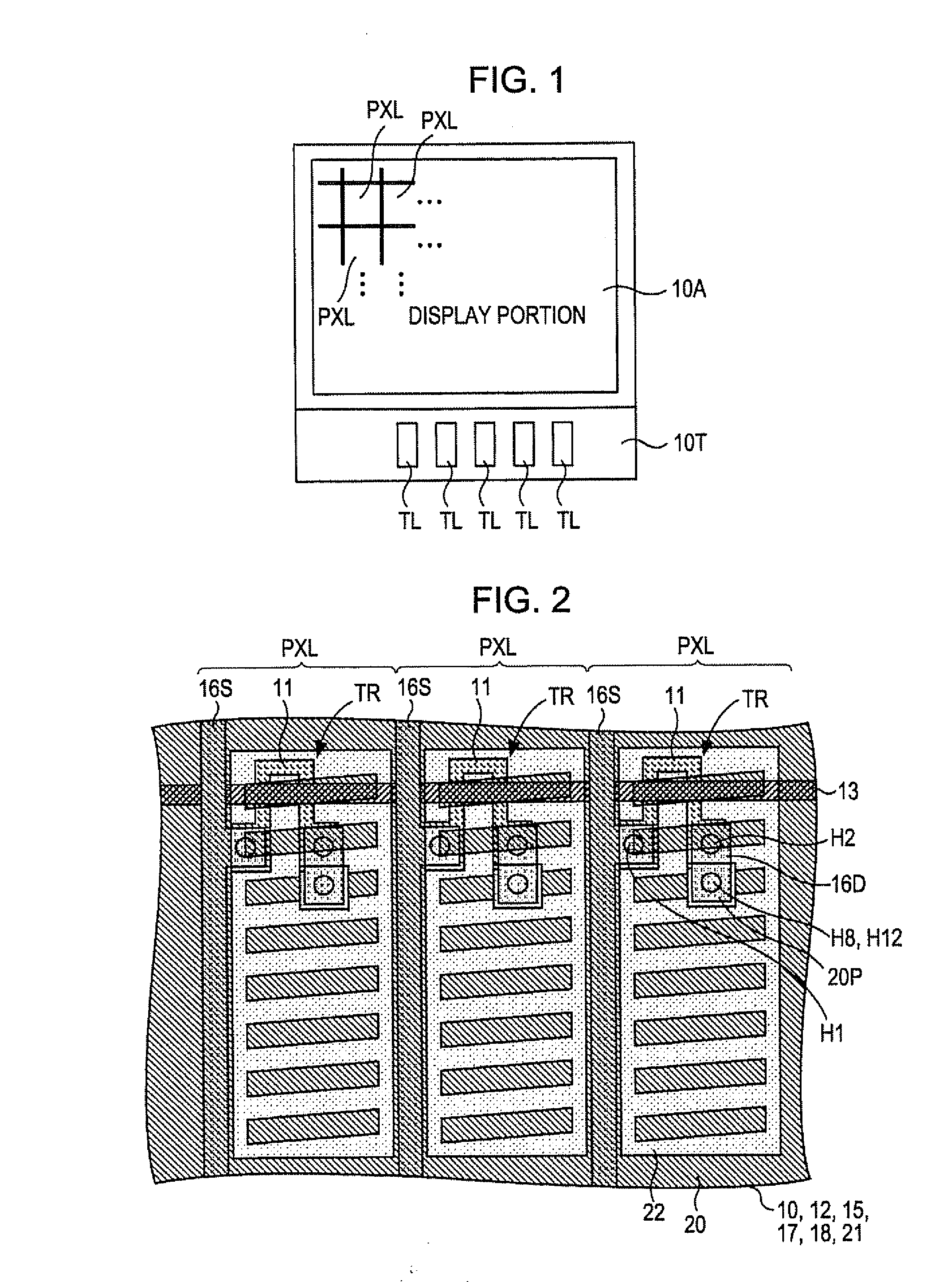
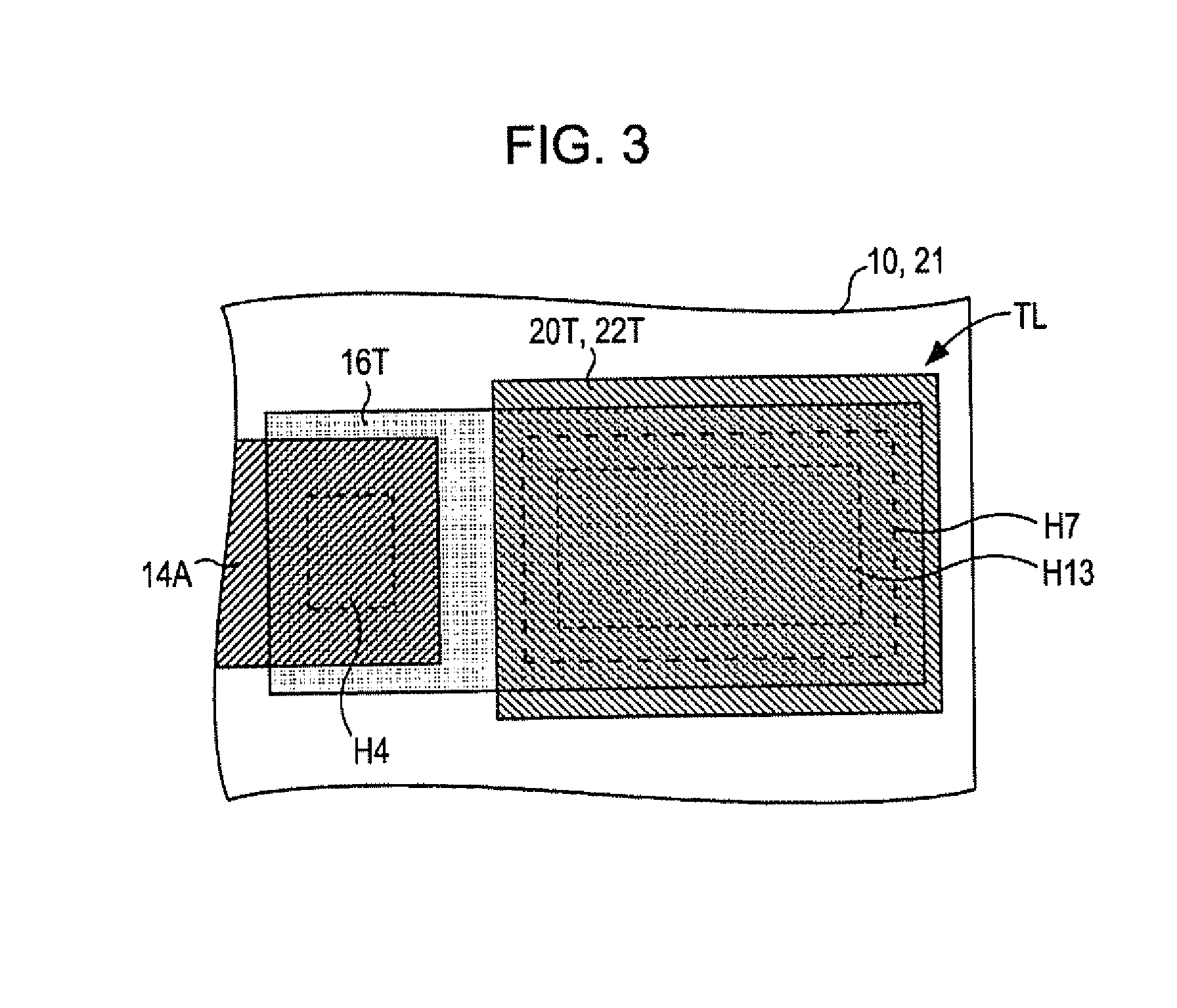
[0033]The planar configuration of a liquid crystal display device according to a first embodiment of the invention will now be described with reference to the accompanying drawings. FIG. 1 is a plan view that shows the schematic configuration of the liquid crystal display device according to the present embodiment. In addition, FIG. 2 is an enlarged plan view of only three pixels PXL from among a plurality of pixels PXL that are formed in a display portion 10A shown in FIG. 1. FIG. 2 shows the configuration that operates in an FFS mode. FIG. 3 is an enlarged plan view of one of a plurality of terminals TL of a terminal portion 10T shown in FIG. 1. FIG. 1 to FIG. 3 only show major components for the sake of convenience of description.

[0034]Note that, in the following description regarding the planar configuration, a gate insulating film 12, an interlayer insulating film 15, a passivation film 17 and a planarization film 18 are also referred to in order to supplement the configuration...


PUM

PropertyMeasurementUnit
thicknessaaaaaaaaaa
temperatureaaaaaaaaaa
electric fieldaaaaaaaaaa

Abstract

A liquid crystal display device comprising: a switching element that has a drain electrode and that is arranged on a substrate; a first insulating film that covers the switching element and that has a first opening on the drain electrode; a first etching stopper electrode that is formed in the first opening and that is connected to the drain electrode; a common electrode that is arranged on the first insulating film; a second insulating film that covers the first etching stopper electrode and the common electrode, and that has a second opening on the first etching stopper electrode; and a pixel electrode that is connected through the second opening to the first etching stopper electrode and that extends onto the second insulating film so as to face the common electrode.

Description

BACKGROUND[0001]1. Technical Field[0002]The present invention relates to a liquid crystal display device and a method of manufacturing the liquid crystal display device and, more particularly, to a liquid crystal display device that controls a liquid crystal using an electric field that is substantially horizontal with respect to a transparent substrate and a method of manufacturing the liquid crystal display device.[0003]2. Related Art[0004]Liquid crystal display devices that use an electric field substantially horizontal with respect to a transparent substrate, that is, liquid crystal display devices that operate in a Fringe-Field Switching (FFS) mode, an In-Plain Switching (IPS) mode, or the like, are known as the liquid crystal display devices that have high contrast and wide viewing angle.[0005]In these liquid crystal display device, pixel electrodes, each of which is supplied with a display signal, and common electrodes that are supplied with a common electric potential both a...

Claims


Application Information

Patent Timeline
Patent Type & Authority Applications(United States)
IPC IPC(8): G02F1/136
CPCG02F1/134363G02F2001/134372G02F1/136227G02F1/13458G02F1/134372G02F1/13439
Inventor AOTA, MASAAKIISHIDA, SATOSHI
Owner JAPAN DISPLAY WEST
Why Eureka
Try Eureka