

Lithography system, method of clamping and wafer table
a technology of lithography and clamping, applied in the field of lithography system, can solve the problems of increasing the complexity of a required, positioning distortion, and disadvantage, and achieve the effect of reducing the negative effect of positioning accuracy of the carrying means
- Summary
- Abstract
- Description
- Claims
- Application Information
AI Technical Summary
Benefits of technology
Problems solved by technology
Method used
Image

Examples
Embodiment Construction
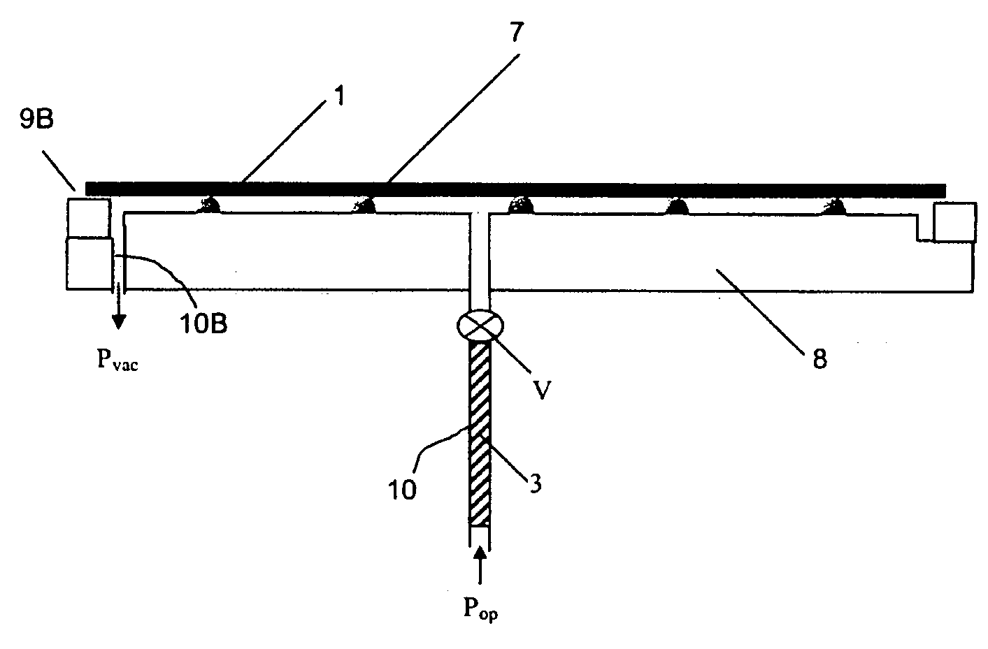
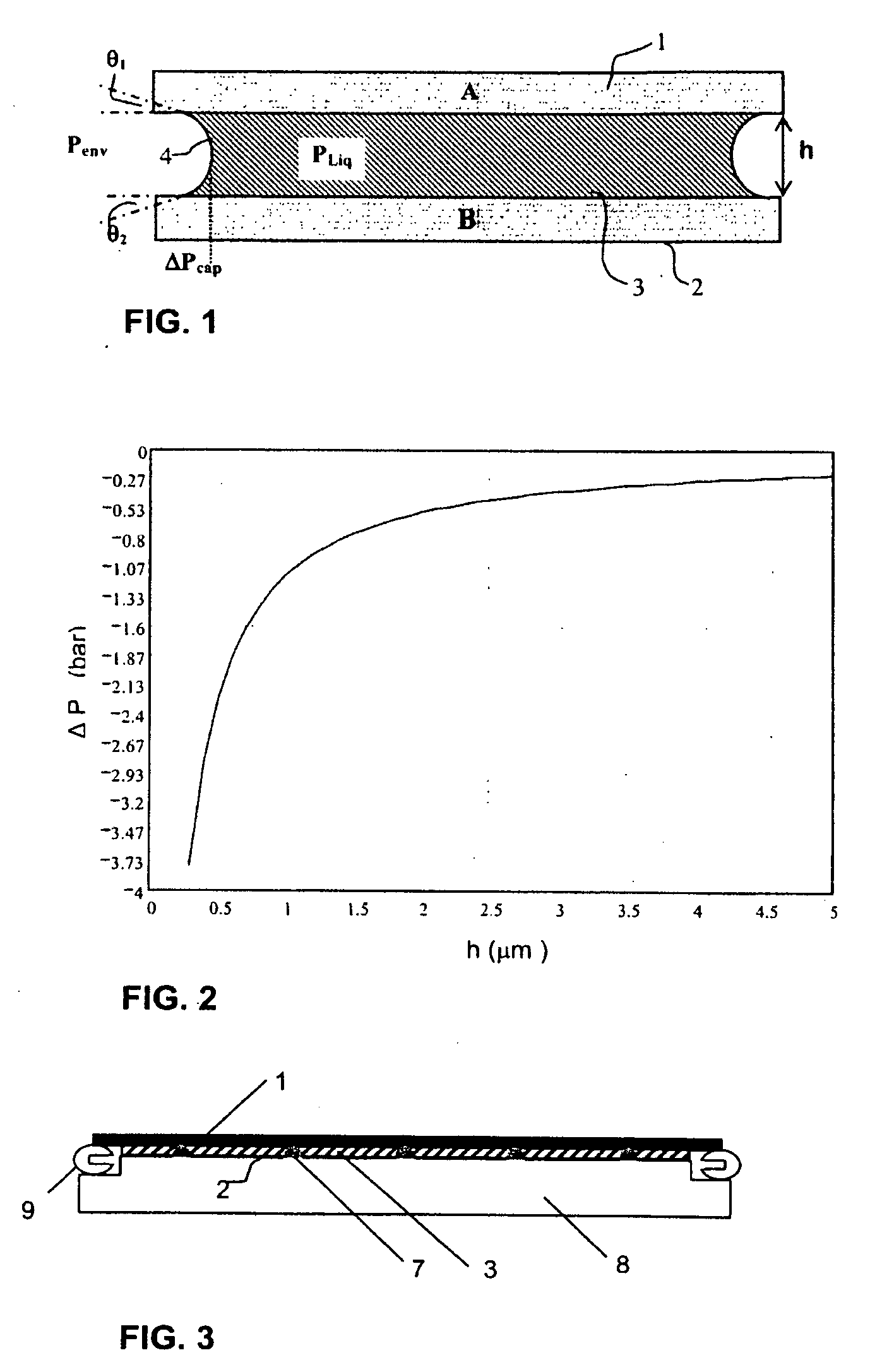
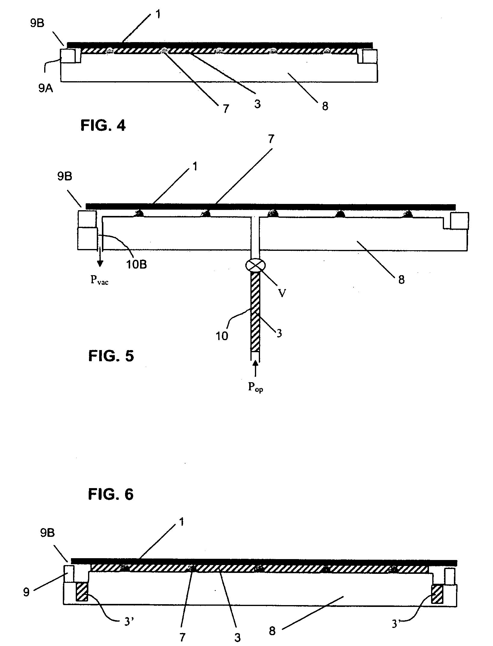
[0033]FIG. 1 shows a lithography target, here in the form of a wafer 1, which normally moves relative to e.g. a charged particle beam column of a litho apparatus, or other kind of beam source for lithography, by means of an actuated target table or chuck, not indicated in this drawing. Between a top side of such target table 2 and said target 1, a volume of liquid 3 in included capillary. To this end the target 1 and top surface 2 have a mutual nominal distance of gap height h. The volume of liquid, according to the invention preferably water, is such that the radius of the target, as taken in top view, is virtually met by a radius R of the capillary included liquid 3. In any case, the radius of an incircle of the target is at least met by the radius of an excircle fitting the volume of liquid within the boundary of the target. In fact, the liquid is to remain, preferably only with a small distance thereto, within the boundaries of the target. The thus included liquid 3 forms a liqu...
PUM
 Abstract
Description
Claims
Application Information