Method for manufacturing photoelectric conversion device

a technology of photoelectric conversion and manufacturing method, which is applied in the direction of sustainable manufacturing/processing, final product manufacturing, coatings, etc., can solve the problems of low productivity, inapplicability, and low deposition rate of microcrystalline silicon film by high-frequency plasma cvd method, so as to reduce the rate of deterioration of characteristics by light degradation and save resources. , the effect of high quality

Inactive Publication Date: 2009-01-29
SEMICON ENERGY LAB CO LTD
View PDF42 Cites 351 Cited by
  • Summary
  • Abstract
  • Description
  • Claims
  • Application Information

AI Technical Summary

Benefits of technology

[0013]According to the present invention, pressure at the time of forming a microcrystalline semiconductor film is set at an atmospheric pressure or a subatmospheric pressure and microwave plasma is generated; therefore, the microcrystalline semiconductor film can be formed at a deposition rate of about 50 times as high as a conventional one and a microcrystalline semiconductor with high quality can be obtained. By forming a photoelectric conversion layer using such a microcrystalline semicond...

Problems solved by technology

In order to use microcrystalline silicon as a photoelectric conversion layer, the thickness of the microcrystalline silicon needs to be equal to or greater than 1 μm, preferably about 10 μm; however, the deposition rate of a microcrystalline silicon film by a high-frequency plasma CVD method is equal to or less than 0.1 nm/sec. even ...

Method used


Image

  • Method for manufacturing photoelectric conversion device
  • Method for manufacturing photoelectric conversion device
  • Method for manufacturing photoelectric conversion device

Examples


Embodiment Construction

[0030]Hereinafter, an embodiment mode of the present invention will be described with reference to the accompanying drawings. Note that the present invention is not limited to the following description and it will be readily appreciated by those skilled in the art that modes and details can be modified in various ways without departing from the spirit and the scope of the present invention. Accordingly, the present invention should not be construed as being limited to the description of the embodiment mode to be given below. Note that same portions in the drawings may be denoted by the same reference numerals in a structure of the present invention to be given below.

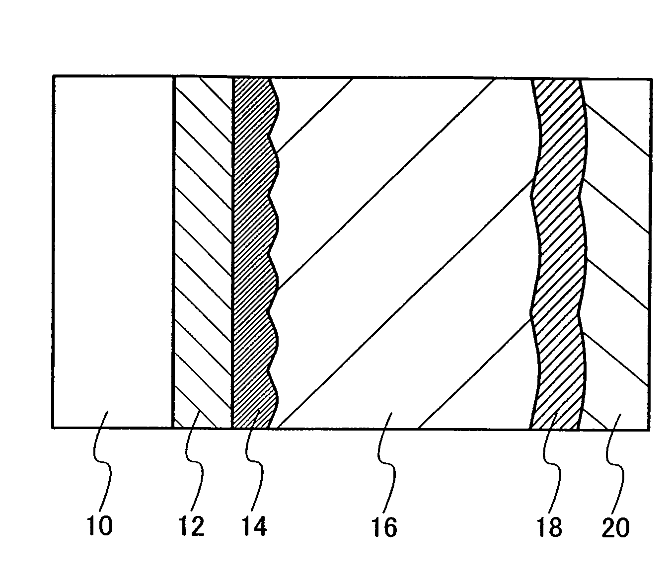
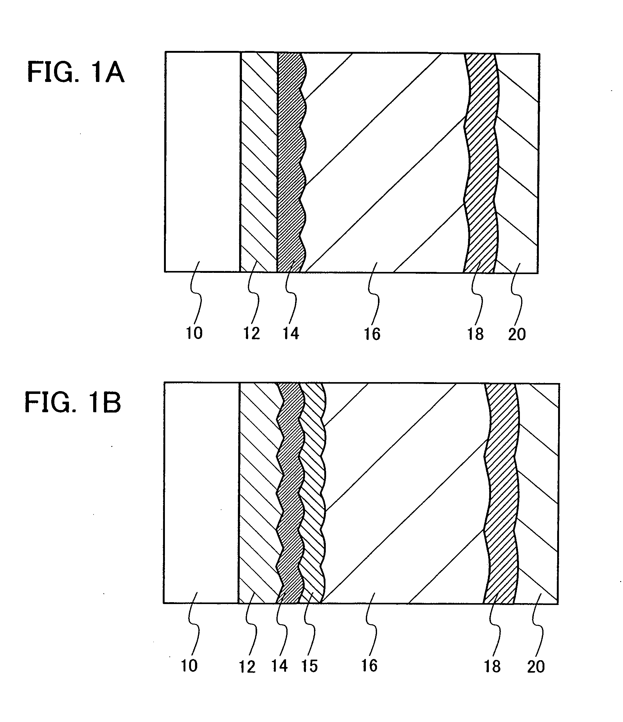
[0031]FIG. 1A illustrates a structure of a photoelectric conversion device of this embodiment mode. The photoelectric conversion device includes at least one semiconductor junction by providing an i-type semiconductor layer 16 between a p-type semiconductor layer 14 and an n-type semiconductor layer 18. In this embodimen...


PUM


Abstract

To form a microcrystalline semiconductor with high quality which can be directly formed at equal to or less than 500° C. over a large substrate with high productivity without decreasing a deposition rate. In addition, to provide a photoelectric conversion device which employs the microcrystalline semiconductor as a photoelectric conversion layer. A reactive gas containing helium is supplied to a treatment chamber which is surrounded by a plurality of juxtaposed waveguides and a wall, the pressure in the treatment chamber is maintained at an atmospheric pressure or a subatmospheric pressure, microwave is supplied to a space sandwiched between the juxtaposed waveguides to generate plasma, and a photoelectric conversion layer of a microcrystalline semiconductor is deposited over a substrate which is placed in the treatment chamber.

Description

BACKGROUND OF THE INVENTION[0001]1. Field of the Invention[0002]The present invention relates to a method for manufacturing photoelectric conversion devices using a microcrystalline semiconductor as a photoelectric conversion layer.[0003]2. Description of the Related Art[0004]To deal with global environmental issues in recent years, the market for photoelectric conversion devices such as residential photovoltaic systems has expanded. As photoelectric conversion devices, devices using a single-crystal or polycrystalline silicon wafer which has high conversion efficiency have been used in practice. The photoelectric conversion devices are manufactured using single-crystal or polycrystalline silicon which is cut out from a large silicon ingot. However, it takes a long time to manufacture large silicon ingots, which deteriorates productivity, and since the supply of silicon raw materials is limited, the supply of silicon ingots is insufficient and cannot deal with the expansion of the m...

Claims


Application Information

Patent Timeline
IPC IPC(8): H01L31/18
CPCC23C16/45561C23C16/45574C23C16/511Y02E10/548H01L31/075H01L31/1824Y02E10/545H01L31/03921Y02P70/50
Inventor ARAI, YASUYUKIYAMAZAKI, SHUNPEI
Owner SEMICON ENERGY LAB CO LTD
Why Eureka
Try Eureka