Liquid crystal display device and manufacturing method thereof

a technology of liquid crystal display and liquid crystal, which is applied in the direction of non-linear optics, instruments, optics, etc., can solve the problems of substrate displacement from each other, occurrence of spots, and long time it takes to inject liquid crystal, so as to prevent poor curing of sealing members and reduce light irradiation energy , the effect of improving manufacturing efficiency

Inactive Publication Date: 2009-02-05
SHARP KK
View PDF6 Cites 32 Cited by
  • Summary
  • Abstract
  • Description
  • Claims
  • Application Information

AI Technical Summary

Benefits of technology

[0025]According to the above method, before forming the sealing member in the first substrate, the transparent film is formed at least on the light blocking section (A) disposed on the opposed surface of the first substrate. Accordingly, the light-blocked region does not emerge in the sealing member but emerges within the transparent film when light is irradiated so as to cure the sealing member. With this, the light is so refracted as to reach the sealing member, with the result that the sealing member is irradiated with light sufficiently. Accordingly, unlike the conventional techniques, it is not necessary to irradiate the light for a long time so as to prevent poor curing of

Problems solved by technology

However, it takes a long time to inject the liquid crystal upon manufacturing the liquid crystal display device in the manner described above.
However, in the above method, when the liquid crystal and the sealing member uncured meet, an ingredient of the sealing member is melt into the liquid crystal.
This results in occurrence of spots.
Further, heat application required in curing the sealing member causes thermal expansion of the array subs

Method used


Image

  • Liquid crystal display device and manufacturing method thereof
  • Liquid crystal display device and manufacturing method thereof
  • Liquid crystal display device and manufacturing method thereof

Examples


first preferred embodiment

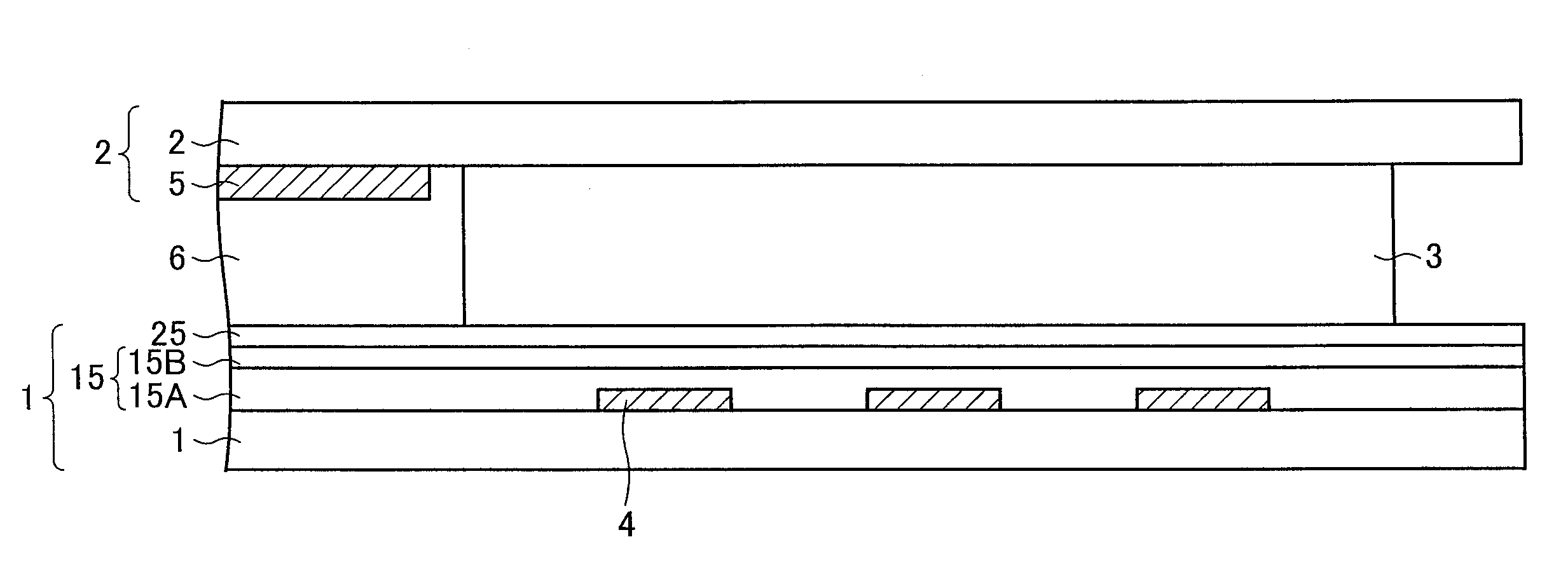
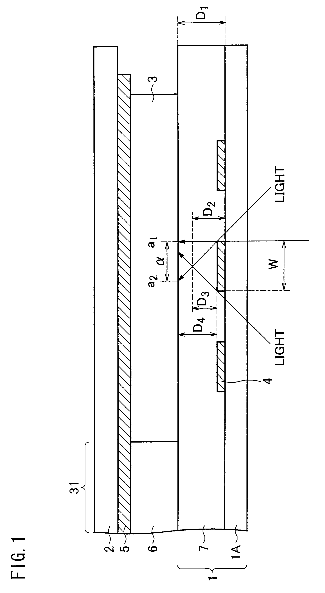
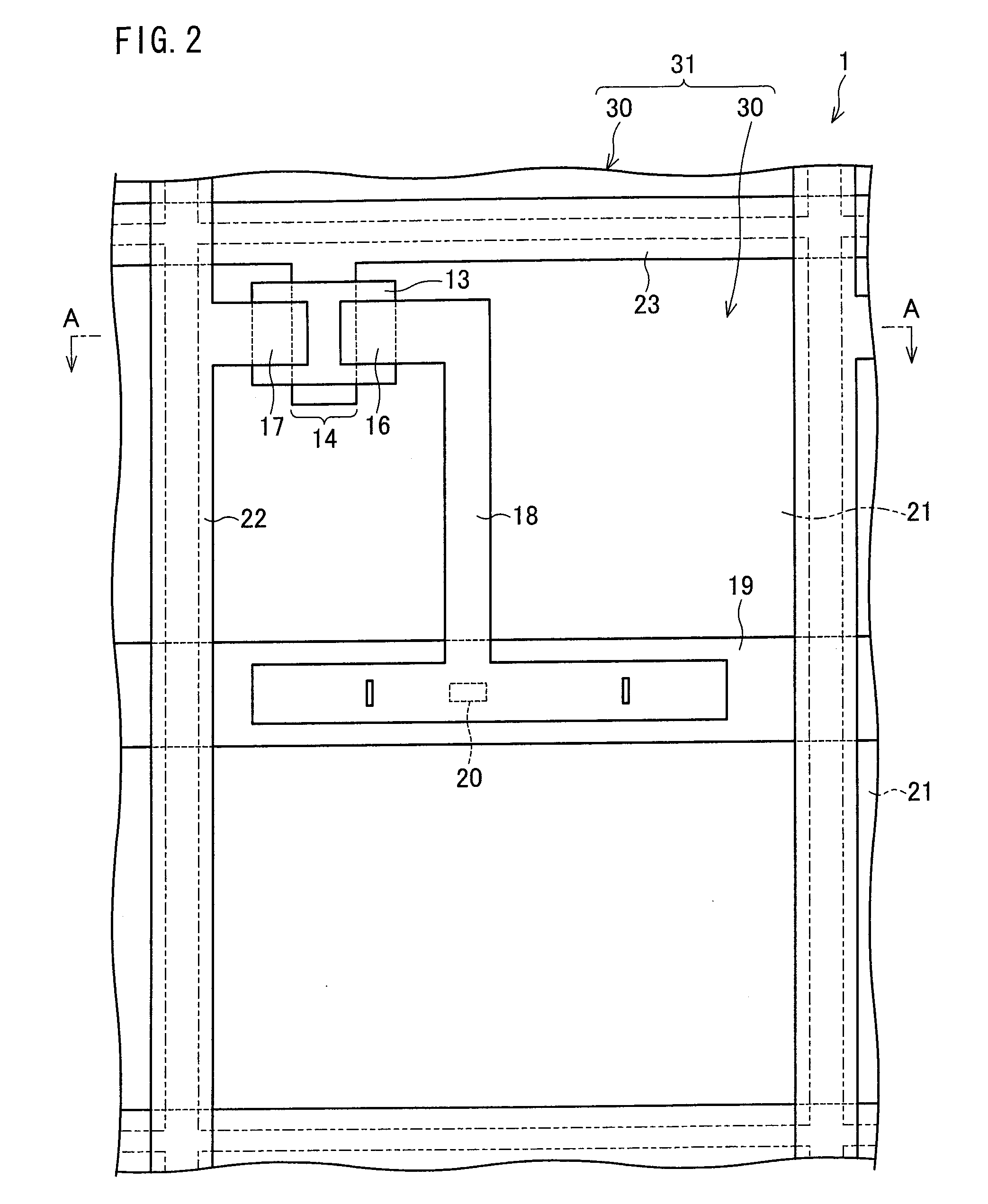
[0046]One preferred embodiment of the present invention will be explained with reference to FIG. 1 to FIG. 4. FIG. 1 is a cross sectional view schematically illustrating the structure of main parts of a liquid crystal display device according to the present preferred embodiment. The liquid crystal display device according to the present preferred embodiment has a panel section whose schematic structure viewed from a flat plane is basically the same as shown in FIG. 8, so that a plan view of the panel section thereof is omitted in the present preferred embodiment. The cross section shown in FIG. 1 is equivalent to the cross section of the liquid crystal display device taken along the line B-B of FIG. 8. Illustration of terminal sections is omitted in FIG. 1. FIG. 2 is a plan view schematically illustrating the structure of an array substrate. FIG. 3 is a cross sectional view illustrating the array substrate shown in FIG. 2 and taken along line A-A. FIG. 4 is a cross sectional view sc...

second preferred embodiment

[0106]Another preferred embodiment of the present invention will be described below with reference to FIG. 5. In FIG. 5, component members equivalent to those shown in the first preferred embodiment are rendered the same reference numerals and detailed explanation therefor is omitted. The present preferred embodiment is the same as the first preferred embodiment, except that a material for the transparent film is not the transparent resin but silicon nitride (SiNx).

[0107]FIG. 5 is a cross sectional view schematically illustrating the structure of main parts of a liquid crystal display device according to the present preferred embodiment. As shown in FIG. 5, in the liquid crystal display device according to the present preferred embodiment, a transparent film 9 is provided between the array substrate 1 and the sealing member 3. The transparent film 9 can be made of a material containing silicon nitride, which is a material used in a general liquid crystal display device. Silicon nitr...

third preferred embodiment

[0115]Still another preferred embodiment of the present invention will be described below with reference to FIG. 6. In FIG. 6, component members equivalent to those shown in the first and second preferred embodiments are rendered the same reference numerals and detailed explanation therefor is omitted. The present preferred embodiment is the same as the second preferred embodiment above, except that the transparent film 9 has a surface on which a section with irregularities is formed. The surface faces the sealing member 3.

[0116]FIG. 6 is a cross sectional view schematically illustrating the structure of main parts of a liquid crystal display device according to the present preferred embodiment. As shown in FIG. 6, a dimple section 8 is formed on the surface of the transparent film 9. In the dimple section 8, irregularities are formed at a pitch of several μm to several ten μm. This makes it possible to refract, in various directions, light entering via the array substrate 1. The li...


PUM


Abstract

In a liquid crystal display device, an array substrate and a CF substrate arranged face to face with each other. A liquid crystal layer is provided between the array substrate and the CF substrate. The array substrate and the CF substrate are bonded together by a sealing member containing a photo curing material. The array substrate has a surface opposed to the CF substrate. Metal wires are provided in the circumferential portion of the opposed surface. A transparent film is disposed between the metal wires and the sealing member.

Description

BACKGROUND OF THE INVENTION[0001]1. Field of the Invention[0002]The present invention relates to a liquid crystal display device and a manufacturing method thereof. Particularly, the present invention relates to a liquid crystal display device using a sealing member containing a photo curing material, and a manufacturing method thereof.[0003]2. Description of the Related Art[0004]Conventionally, liquid crystal display devices have been widely used as substitution for CRTs. The liquid crystal display devices are thinner than the CRTs and can be downsized, so that the liquid crystal display devices are used for mobile terminals such as laptop PCs and mobile phones.[0005]An active matrix type liquid crystal display device of these liquid crystal display devices has been mainly used in recent years. The active matrix type liquid crystal display device is arranged such that an array substrate on which thin film transistors (TFT) are formed in a matrix manner and a CF substrate on which a...

Claims


Application Information

Patent Timeline
IPC IPC(8): G02F1/1333G02F1/1339
CPCG02F1/1333G02F1/1339G02F1/133514
Inventor YAMADA, NAOSHITSUBATA, TOSHIHIDEYAMAGUCHI, HIDEHIKOSHIMADA, YOSHINORI
Owner SHARP KK
Why Eureka
Try Eureka