Nonvolatile memory device having a plurality of memory blocks

a technology of nonvolatile memory and memory blocks, which is applied in the direction of static storage, digital storage, instruments, etc., can solve the problems of not revealing the related configurations of power source lines, the negative voltage of 9v/9v produces an extremely large power source noise with respect to sensitivity, and the voltage fluctuations caused by the rewrite operation may become a noise source with respect to the read operation, so as to prevent voltage fluctuations, prevent interference between the read operation and the rewri

Active Publication Date: 2009-02-05
INFINEON TECH LLC
View PDF3 Cites 7 Cited by
  • Summary
  • Abstract
  • Description
  • Claims
  • Application Information

AI Technical Summary

Benefits of technology

[0015]In the nonvolatile memory device according to the present invention, the power sources of the first voltage generating unit and the rewrite memory block, and the sense amplifier and the read memory block are each supplied with power supply voltages or/and ground voltages that differ from each another. This makes it possible to prevent voltage fluctuations associated with charging/discharging of a boost voltage or/and negative voltage carried out under the control of the first voltage generating unit and the rewrite block from influencing the sense amplifier and the read memory block. Thus, the read operation can be reliably carried out even in the event the rewrite operation...

Problems solved by technology

In addition, the related art does not describe the power source lines for supplying a power source voltage or/and ground lines in a circuit for carrying out a rewrite operation of erasing/writing, as an internal operation, and a circuit for carrying out an operation to read out data to the exterior, and does not disclose the related configurations of the power source lines or/and ground lines.
If the read operation in which a micro-signal must be amplified by a sense amplifier and the rewrite operation in which a boost voltage or/and negative voltage must be generated and a rewrite high-voltage stress is applied to a memory cell are carried out simultaneously, a problem arises that voltage fluctuations caused by the rewrite operation may become a noise source with respect to the read operation.
F...

Method used


Image

  • Nonvolatile memory device having a plurality of memory blocks
  • Nonvolatile memory device having a plurality of memory blocks
  • Nonvolatile memory device having a plurality of memory blocks

Examples


Embodiment Construction

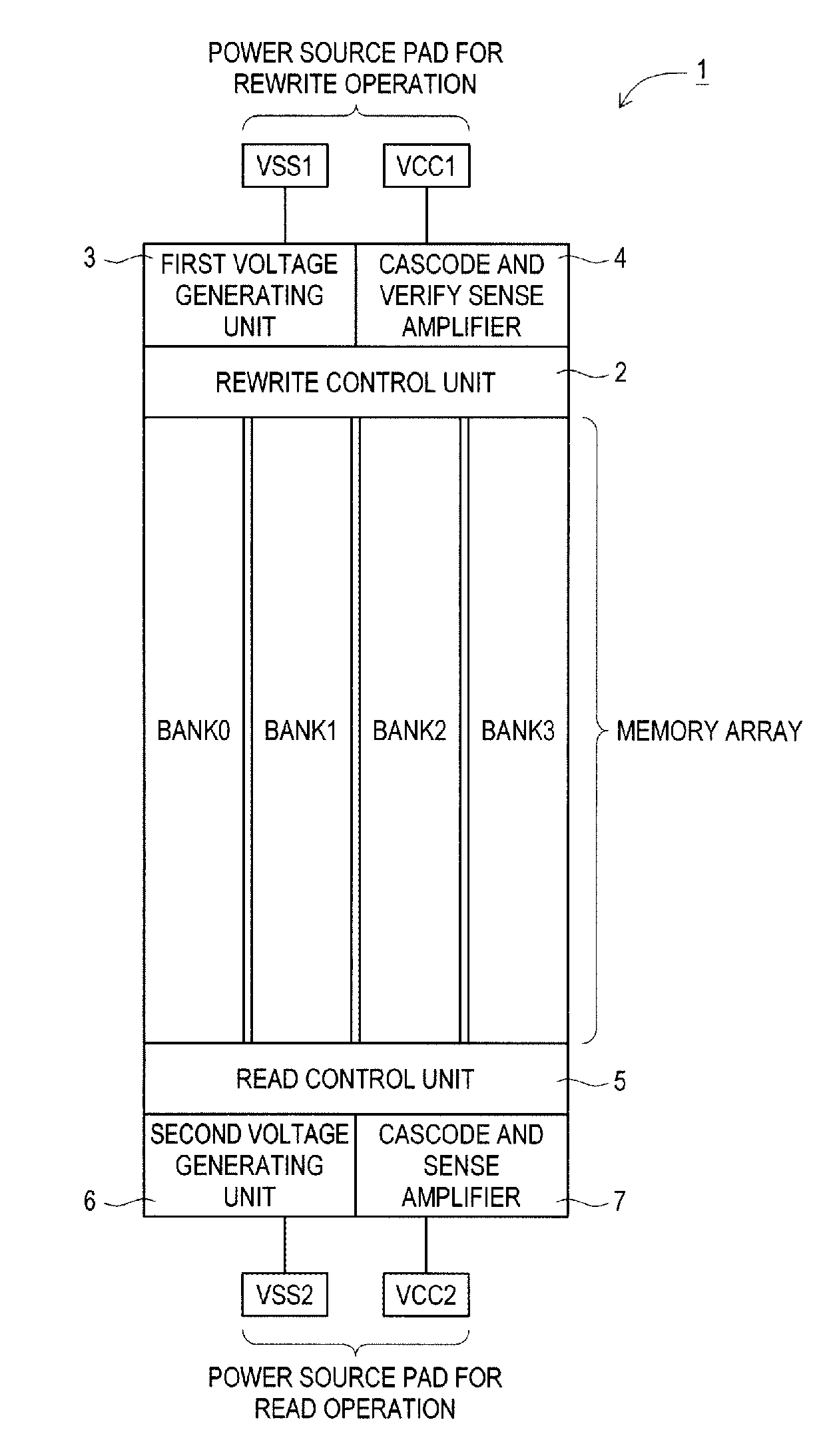
[0024]Referring to FIG. 1, a configuration diagram showing the layout of a nonvolatile memory device 1 according to the embodiment is depicted. The non-volatile memory device 1 comprises banks 0 through 3 in a memory array, and is capable of reading from a bank other than a predetermined bank while rewriting to the predetermined bank, in other words, it is capable of accommodating Simultaneous Operation (SO).

[0025]The nonvolatile memory device 1 comprises a rewrite control unit 2 arranged at an upper side of the memory array, and a read control unit 5 arranged at a lower side of the memory array.

[0026]Further, a first voltage generating unit 3 and a cascode amplifier and a verify sense amplifier 4 are arranged above the rewrite control unit 2. The power source lines and the ground lines of the rewrite control unit 2, and the first voltage generating unit 3, as well as the cascode amplifier and the verify sense amplifier 4 are connected to the first power source line VCC1 and the fir...


PUM


Abstract

A nonvolatile memory device 1 capable of preventing interference between a read operation and a rewrite operation, and capable of preventing malfunctions that may occur in the event the read operation and the rewrite operation are performed simultaneously between memory blocks is provided. The nonvolatile memory device 1 is provided with a plurality of banks, a rewrite control unit 2 to which a first power source line VCC1 and a first ground line VSS1 are connected and which is adapted to control a rewrite operation with respect to a bank i, and a read control unit 5 to which a second power source line VCC2 and a second ground line VSS2 are connected and which is adapted to control a read operation with respect to a bank j, wherein the rewrite control unit 2 and the read control unit 5 are arranged so as to be spaced from each another.

Description

CROSS-REFERENCE TO RELATED APPLICATIONS[0001]The present invention is based on Japanese Patent Application No. 2007-194277 filed on Jul. 26, 2007, the disclosure of which is hereby incorporated by reference.TECHNICAL FIELD[0002]The invention relates to nonvolatile memory devices having a plurality of memory blocks and, more particularly, relates to a nonvolatile memory device in which read access operations and rewrite access operations with applied voltages differing from each other are carried out asynchronously with respect to each of a plurality of memory blocks.BACKGROUND OF THE INVENTION[0003]In a nonvolatile semiconductor memory device disclosed in Japanese Patent Application Publication No. 2001-344986, an external read Y gate YGE and an internal operation Y gate YGI are arranged opposite to each other at opposite sides in the column direction of a memory cell array MA in each bank. The external read Y gate YGE couples a selected column of the memory cell array MA with the e...

Claims


Application Information

Patent Timeline
IPC IPC(8): G11C16/12
CPCG11C16/12
Inventor FURUYAMA, TAKAAKINIIMI, MAKOTONIIMI, MASAHIRO
Owner INFINEON TECH LLC
Why Eureka
Try Eureka