

Photoresist Composition for Deep UV and Process Thereof
a technology of photoresist and composition, applied in the field of photoresist composition, can solve the problems that open-chain aliphatic resins the material applicable for photoresist at 248 nm cannot be used at 193 nm, and the effect of affecting the performance of photoresis
- Summary
- Abstract
- Description
- Claims
- Application Information
AI Technical Summary
Benefits of technology
Problems solved by technology
Method used
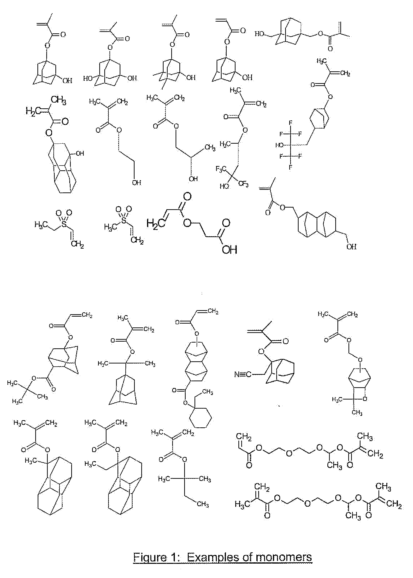
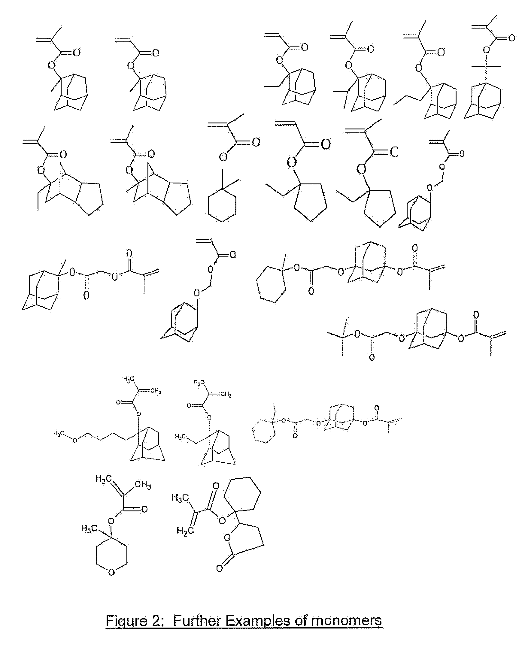
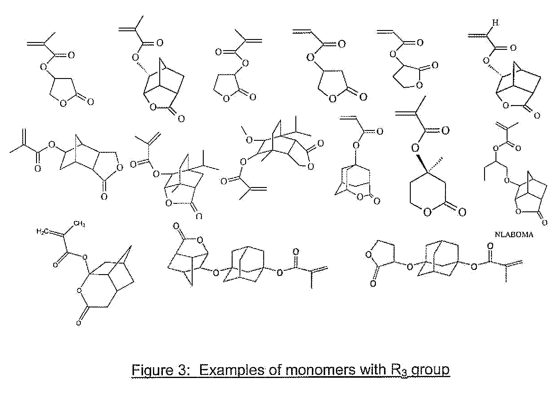
Image

Examples
example 1
COMPARATIVE PHOTORESIST EXAMPLE 1
[0090]1.2151 g of Poly(EAdMA / ECPMA / HAdA / a-GBLMA) 15 / 15130140 polymer made in polymer synthesis example (1), 0.0282 g of bis(p-tertbutyl phenyl)iodonium perfluoroethanesulfonylimide (BDPINC2), 0.0323 g of bis(triphenylsulfonium) perfluorobutane-1,4-disulfonate, (TPSC4), 0.0655 grams of bis(p-tertiarybutylphenyl)iodonium perfluorobutane-1,4-disulfonate, 0.0071 grams of N,N-diisopropylaniline, 0.0018 g of phenyl-N,N-diethanolamine, 0.0036 grams of FC4430 surfactant supplied by 3M Corporation Were dissolved in 22.6545 g of methylalphahydroxyisobutyrate (MHIB) and 5.6007 g of propyleneglycolmonomethylether and 0.3912 g of gamma valerolactone. The solution was thoroughly mixed for complete dissolution and filtered using 0.2 um filter.
[0091]A silicon substrate coated with a bottom antireflective coating (B.A.R.C.) was prepared by spin coating the bottom anti-reflective coating solution (AZ® ArF-38, B.A.R.C. available from AZ® Electronic Materials Corporatio...
example 2
COMPARATIVE PHOTORESIST EXAMPLE 2
[0092]2.9049 g of Poly(EAdMA / HAdA / a-GBLA) 50 / 20 / 30 polymer made in polymer synthesis example (2), 0.0549 g of triphenylsulfonium perfluoropropanesulfonylimide (TPS_PFSI_Cy6), 0.0258 g of bis(triphenylsulfonium) perfluorobutane-1,4-disulfonate, (TPSC4), 0.0145 g of tris[2-(2-methoxyethoxy)ethyl]amine, 0.0060 grams of FC4430 surfactant supplied by 3M Corporation were dissolved in 46.9940 g of a 60 / 40 (w / w) mixture of propyleneglycol monomethylether acetate and ethyl lactate. The solution was thoroughly mixed for complete dissolution and filtered using 0.2 um filter.
[0093]A silicon wafer coated with a bottom antireflective coating (B.A.R.C.) was prepared by spin coating the bottom anti-reflective coating solution (AZ® 1C5D, B.A.R.C. available from AZ Electronic Mhaterials Corporation, Somerville, N.J.) onto the silicon substrate and baking at 200° C. for 60 sec. The B.A.R.C film thickness was 37 nm. The photoresist solution prepared in this Example was ...
example 3
PHOTORESIST EXAMPLE 3
[0094]0.012 g of homopolymer of 1,1,2-trifluoro-4-(2,2,2-trifluoro-1-hydroxy-1-trifluoromethylethyl)-1,6-heptadiene (CF2═(═FCH2CH(C(CF3)2(OH))CH2CH═CH2 (TFTFHMH)), that was 70 mole % protected with methoxymethyl group,corresponding to 1 weight percent of polymer (available from Asahi Glass Co., Ltd., 12-1 Yurakucho 1-Chome, Chiyoda-Ku, Tokyo 100-8405, Japan) was mixed with 30 g of photoresist from Comparative Example 1. The resultant mixture was placed on a roller for 8 h and filtered using 0.2 um filter.
[0095]The photoresist of this example was processed in the same manner as described in Comparative Photoresist Example 1. The photoresist had a photosensitivity of 38 mJ / cm2 for printing 70 nm (1:1) trench without mask bias, with a DoF of 0.30 um, and the average 3sigma LER / LWR values at ±0.10 um DoF was 4.88 and 7.17 nm respectively.
[0096]The photoresist of this example had a water static contact of 87.53° and was much higher than that of the Comparative Photor...
PUM
| Property | Measurement | Unit |
|---|---|---|
| contact angle | aaaaa | aaaaa |
| wavelength | aaaaa | aaaaa |
| wavelengths | aaaaa | aaaaa |
Abstract
Description
Claims
Application Information