Semiconductor device and manufacturing method for the same
Inactive Publication Date: 2009-02-26
SEMICON ENERGY LAB CO LTD
View PDF31 Cites 51 Cited by
Summary
Abstract
Description
Claims
Application Information
AI Technical Summary
This helps you quickly interpret patents by identifying the three key elements:
Problems solved by technology
Method used
Benefits of technology
[0019]A semiconductor substrate provided with an integrated circuit is polished by CMP or the like, and the semiconductor substrate is made into a thin film by forming an embrittlement layer in the semiconductor substrate and separating a part of the semiconductor substrate; thus, semiconductor chips such as an IC chip which is thinner than ever can be obtained.
[0020]Further, a semiconductor substrate provided with an integrated circuit such as an LSI is polished by CMP or the like, and t
Problems solved by technology
However, since CMP is a processing technique in which a wafer is pressed against a polishing cloth while supplying an abrasive, the wafer can be processed to have a thickne
Method used
Image
Click on the blue label to locate the original text in one second.
Reading with bidirectional positioning of images and text.
Examples
embodiment modes
[0044]Embodiment Modes of the present invention will be described below with reference to the accompanying drawings. Note that the present invention is not limited to the following description, and it will be readily understood by those skilled art that various changes and modifications are possible, unless such changes and modifications depart from the spirit and the scope of the present invention. Therefore, the present invention should not be construed as being limited to the description of the embodiment modes to be given below. In the structure of the present invention which is described below, the like reference numerals may denote the like parts throughout the different drawings.
embodiment mode 1
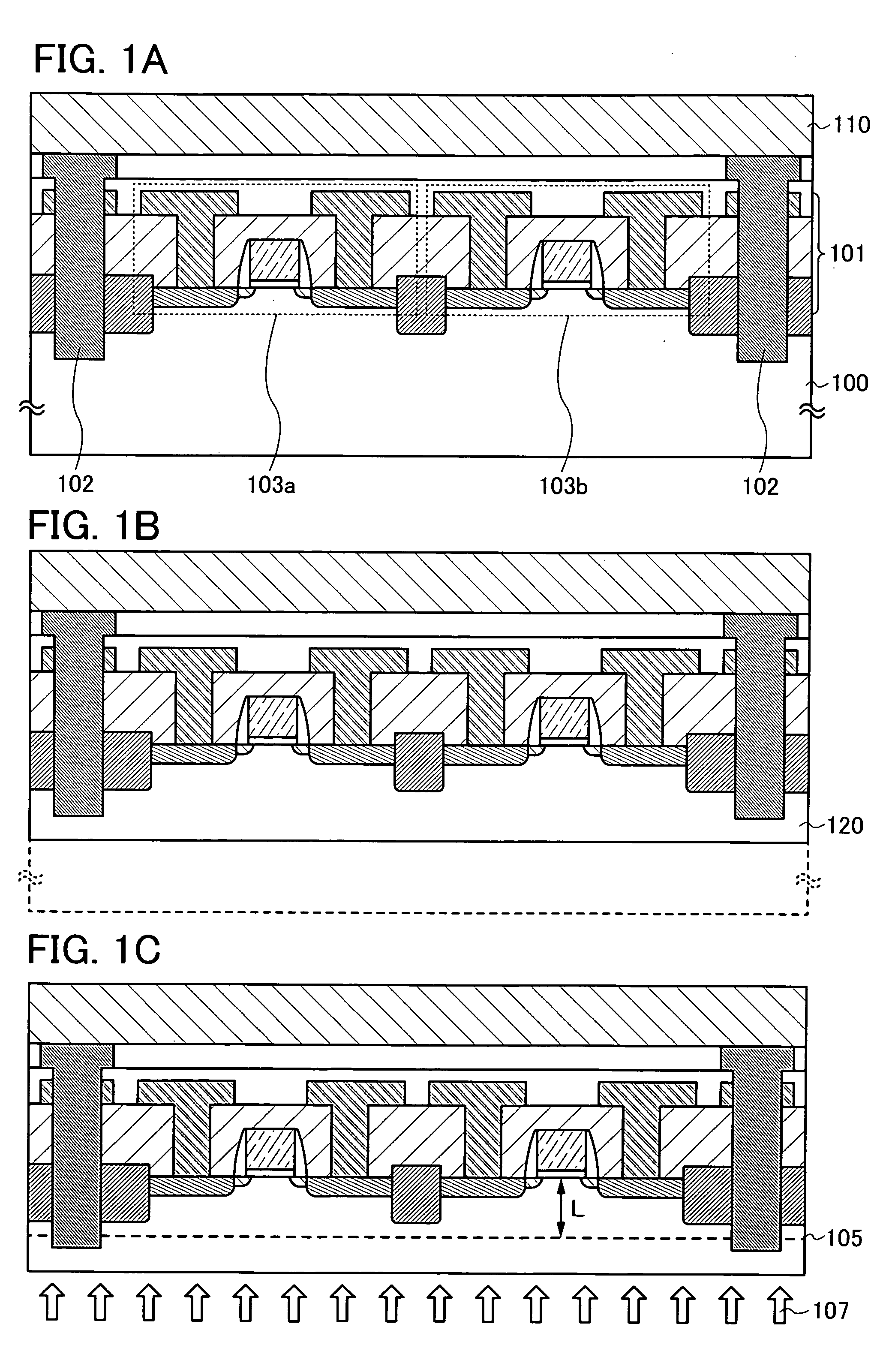
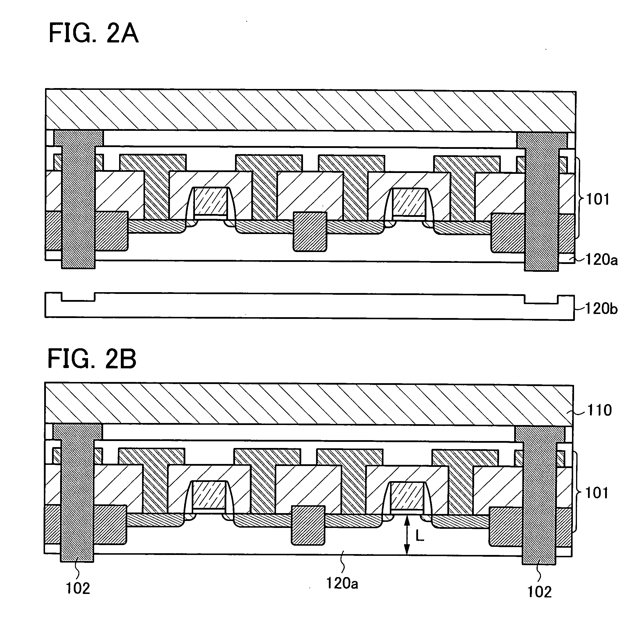
[0045]In this embodiment mode, semiconductor chips such as an IC chip or an LSI chip which have a structure obtained by, after a semiconductor substrate provided with an element formation layer and a through wiring is made into a thin film, separating a part of the semiconductor substrate, will be described with reference to the drawings. Specifically, a semiconductor chip and a method for manufacturing the semiconductor chip will be explained, the semiconductor chip having a structure obtained by, after a semiconductor substrate provided with an element formation layer and a through wiring is made into a thin film, separating a part of the semiconductor substrate, and thereby the through wiring is exposed.
[0046]First, an element formation layer 101, a through wiring 102, and a support substrate 110 are provided over a surface of a semiconductor substrate 100 (see FIG. 1A).
[0047]As the semiconductor substrate 100, a single crystal semiconductor substrate of silicon, germanium, or th...
embodiment mode 2
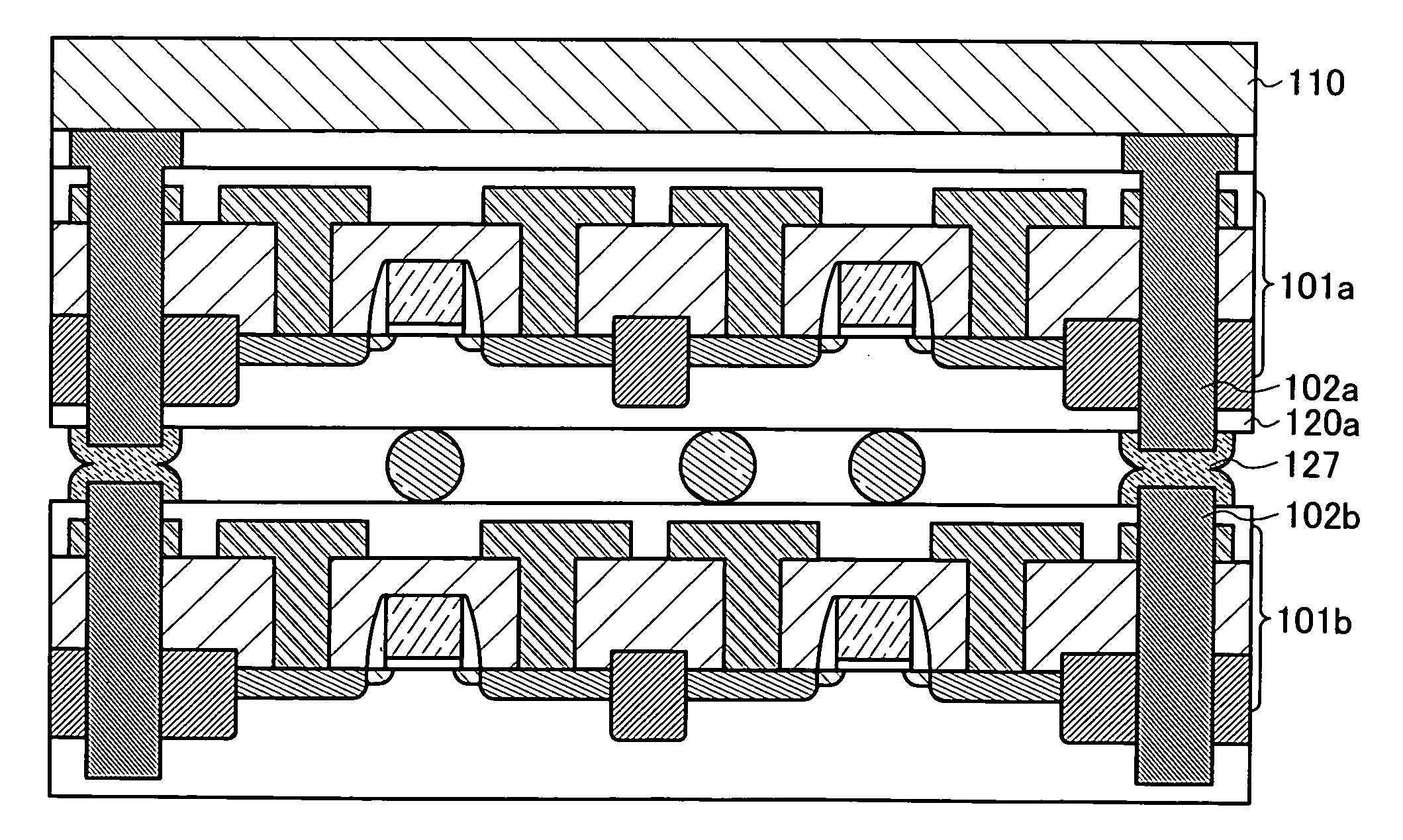
[0059]In this embodiment mode, a semiconductor device having an IC chip provided with a through wiring shown in the above Embodiment Mode 1 will be described with reference to the drawings. Specifically, the case of providing an IC chip on a substrate provided with a wiring so that a through wiring of the IC chip is electrically connected to the wiring will be shown.
[0060]In a semiconductor device shown in FIG. 3A, an IC chip 2130 shown in the above Embodiment Mode 1 is provided by adhesion onto an interposer 2150 provided with a wiring 2152. Here, the element formation layer 101 and the wiring 2152 which are provided in a plurality of IC chips 2130a to 2130d are electrically connected to each other. The element formation layer 101 and the wiring 2152 are connected by electrically connecting the through wiring 102 provided in each of the IC chips 2130a to 2130d and a connection terminal 2151 connected to the wiring 2152 (see FIG. 3B).
[0061]Further, an example of the case of electric...
PUM
Abstract
A semiconductor substrate provided with an integrated circuit is polished by CMP or the like, and the semiconductor substrate is made into a thin film by forming an embrittlement layer in the semiconductor substrate and separating a part of the semiconductor substrate; thus, semiconductor chips such as IC chips and LSI chips which are thinner than ever are obtained. Moreover, such thinned LSI chips are stacked and electrically connected through wirings penetrating through the semiconductor substrate; thus, a three dimensional semiconductor integrated circuit with improved packing density is obtained.
Description
BACKGROUND OF THE INVENTION[0001]1. Field of the Invention[0002]The present invention relates to a semiconductor device including a thinned semiconductor substrate and a method for manufacturing such a semiconductor device. The present invention particularly relates to a semiconductor device having a wiring which penetrates through a thinned semiconductor substrate and a method for manufacturing such a semiconductor device.[0003]2. Description of the Related Art[0004]In various scenes of social life today, information processing is performed using a computer network, and realization of a ubiquitous society where convenience of the processing of information through a computer network can be enjoyed is approaching. The term “ubiquitous” originates from Latin and means “existing everywhere”, which has been used to have the meaning of “information processing utilizing computers is naturally assimilated into our life environment without consciousness of computers”.[0005]Actually, telepho...
Claims
Application Information
Patent Timeline
Application Date:The date an application was filed.
Publication Date:The date a patent or application was officially published.
First Publication Date:The earliest publication date of a patent with the same application number.
Issue Date:Publication date of the patent grant document.
PCT Entry Date:The Entry date of PCT National Phase.
Estimated Expiry Date:The statutory expiry date of a patent right according to the Patent Law, and it is the longest term of protection that the patent right can achieve without the termination of the patent right due to other reasons(Term extension factor has been taken into account ).
Invalid Date:Actual expiry date is based on effective date or publication date of legal transaction data of invalid patent.