Electro-optical Device and Electronic Apparatus

Inactive Publication Date: 2009-02-26
SEIKO EPSON CORP
View PDF1 Cites 8 Cited by
  • Summary
  • Abstract
  • Description
  • Claims
  • Application Information

AI Technical Summary

Benefits of technology

[0009]An advantage of some aspects of the invention is to provide an electro-optical device that has a storage capacitor having a planar structure and is capable of increasing numerical aperture in an easy manner while completely preventing or at least reducing

Problems solved by technology

As a result thereof, there is a risk of a short-circuit failure that could occur between the upper capacitor electrode thereof and the gate electrode.
In addition to such a disadvantage, according to the above-described layer structure, it is practically impossible, or at best difficult, to shut off any incident light beam that propagates toward the semiconductor layer through upper layers formed above the semiconductor layer by means of the upper capacitor electrode.
For this reason, in the planar structure disclosed in the above-identified JP-A-10-10548, it is practically impossible or at best difficult to achieve a small difference between the electric potential of the above-mentioned still another capacitor electrode that is made of the same film as the light-shielding film and the upper-layer capacitor electrode that is made of the same film as the semiconductor layer.
Since it is not possible to achieve a small electric potential difference therebetween, it is practically impossible or at best difficult to make the thickness of a dielectric film small.
Since it is impossible

Method used


Image

  • Electro-optical Device and Electronic Apparatus
  • Electro-optical Device and Electronic Apparatus
  • Electro-optical Device and Electronic Apparatus

Examples


first embodiment

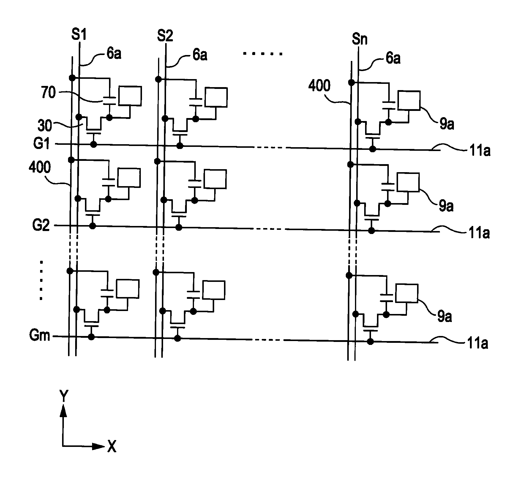
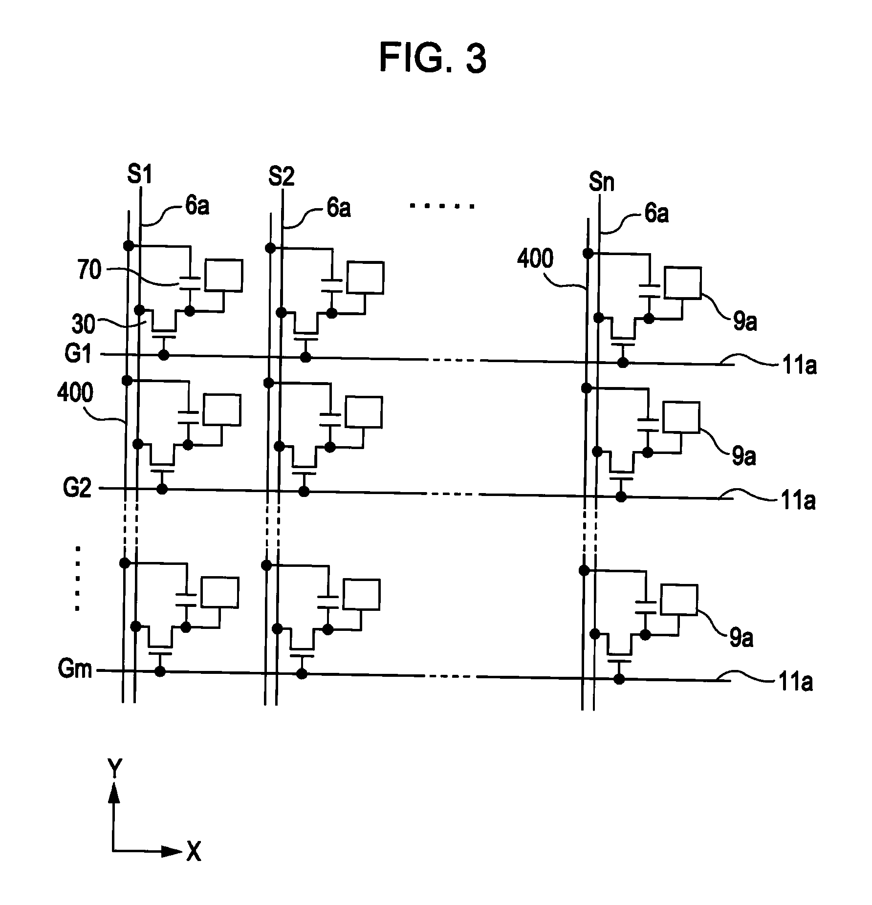
[0056]With reference to FIGS. 1-6, a liquid crystal device according to a first exemplary embodiment of the invention is explained below.

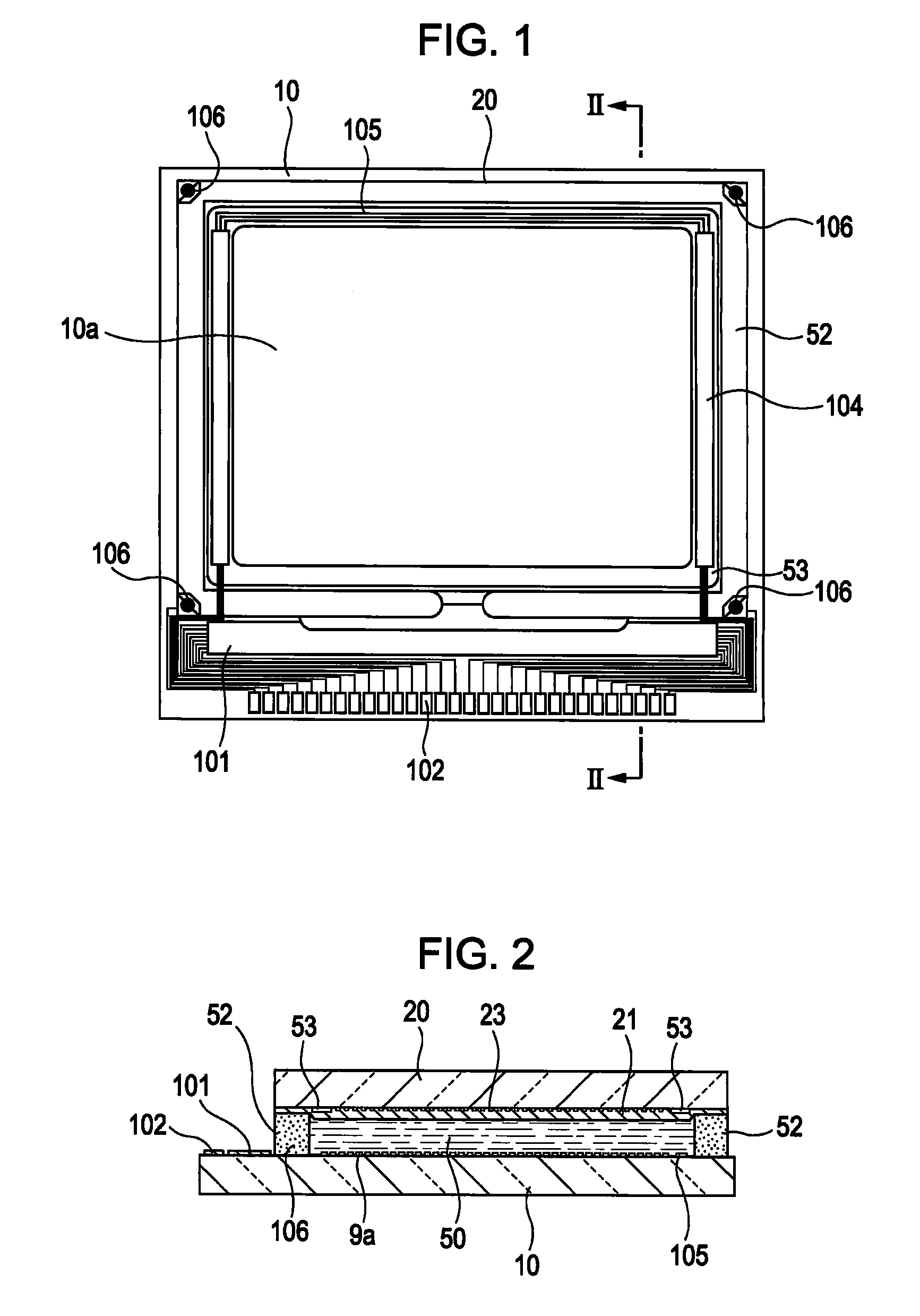
[0057]First of all, an example of the general configuration of a liquid crystal device according to the present embodiment of the invention is explained below while referring to FIGS. 1 and 2. FIG. 1 is a plan view that schematically illustrates an example of the configuration of a TFT array substrate and various components formed or deposited thereon, which are viewed from a certain point at the counter-substrate side, or from above the counter substrate. FIG. 2 is a sectional view taken along the line II-II of FIG. 1.

[0058]As shown in FIGS. 1 and 2, in the configuration of a liquid crystal device according to the present embodiment of the invention, a TFT array substrate 10 and a counter substrate 20 are arranged opposite to each other. The TFT array substrate 10 is a transparent substrate that is made of, for example, a quartz substrate, a glass...

second embodiment

[0108]Next, with reference to FIGS. 7 and 8, a liquid crystal device according to a second exemplary embodiment of the invention is explained below.

[0109]The layer / lamination structure of each pixel of a liquid crystal device according to the second embodiment of the invention differs from the layer / lamination structure of each pixel of a liquid crystal device according to the foregoing first embodiment of the invention in that the former has a dual-layer storage capacitor. The storage capacitor having a dual-layer structure according to the second embodiment of the invention is made up of the second-layer semiconductor film (i.e., semiconductor layer), the third-layer upper capacitor electrode, and the fourth-layer relay electrode. In the following description of a liquid crystal device according to the second embodiment of the invention, differences in the layer / lamination structure thereof from that of the liquid crystal device according to the first embodiment of the invention d...

third embodiment

[0119]Next, with reference to FIG. 10, a liquid crystal device according to a third exemplary embodiment of the invention is explained below.

[0120]The layer / lamination structure of each pixel of a liquid crystal device according to the third embodiment of the invention differs from the layer / lamination structure of each pixel of a liquid crystal device according to the foregoing first embodiment of the invention and the layer / lamination structure of each pixel of a liquid crystal device according to the foregoing second embodiment of the invention in that, in the configuration of a liquid crystal device according to the third embodiment of the invention described below, one storage capacitor is formed above the planar storage capacitor(s) of a liquid crystal device according to the foregoing first embodiment of the invention or the foregoing second embodiment of the invention. More specifically, in the configuration of a liquid crystal device according to the third embodiment of the...


PUM


Abstract

An electro-optical device includes a plurality of storage capacitors each in a corresponding pixel. Each storage capacitor includes a first capacitor electrode and a second capacitor electrode with a dielectric film therebetween. The first capacitor electrode is made of the same film as one of the semiconductor films in pixel transistors. The second capacitor electrode is provided at a layer over the gate electrode of the pixel transistors. The second capacitor electrode has a first main portion opposite to the first capacitor electrode and an extending portion that extends from the first main portion to at least partially cover the second junction region. An interlayer insulation film insulates the extending portion from the pixel transistor.

Description

BACKGROUND[0001]1. Technical Field[0002]The present invention relates to an electro-optical device suck as a liquid crystal device or the like. In addition, the invention further relates to an electronic apparatus that is provided with an electro-optical device. An example of a variety of electronic apparatuses to which the invention can be applied includes but not limited to a liquid crystal projector.[0003]2. Related Art[0004]In a typical configuration of an electro-optical device of the related art, a pixel electrode is provided at an open region of each pixel, whereas a transistor that functions as a switching element for switch-controlling the pixel electrode and a storage capacitor that temporarily retains / holds the electric potential of the pixel electrode are formed in a non-open region of each pixel. In a lamination structure formed over a substrate according to the configuration of an electro-optical device disclosed in JP-A-2005-45017 or Japanese Patent No. 3,141,860, a s...

Claims


Application Information

Patent Timeline
IPC IPC(8): G02F1/133
CPCG02F2202/10G02F1/136213
Inventor YASUKAWA, MASAHIRO
Owner SEIKO EPSON CORP
Why Eureka
Try Eureka