

Method and apparatus for monitoring plasma-induced damage using DC floating potential of substrate
a technology of plasma-induced damage and floating potential, which is applied in the direction of semiconductor/solid-state device testing/measurement, instruments, coatings, etc., can solve the problems of changing the voltage applied to the substrate, none of these methods directly measure the substrate dc voltage, etc., and achieve the effect of detecting substrate damage more accurately
- Summary
- Abstract
- Description
- Claims
- Application Information
AI Technical Summary
Benefits of technology
Problems solved by technology
Method used
Image

Examples
example 1
(Overall Configuration)
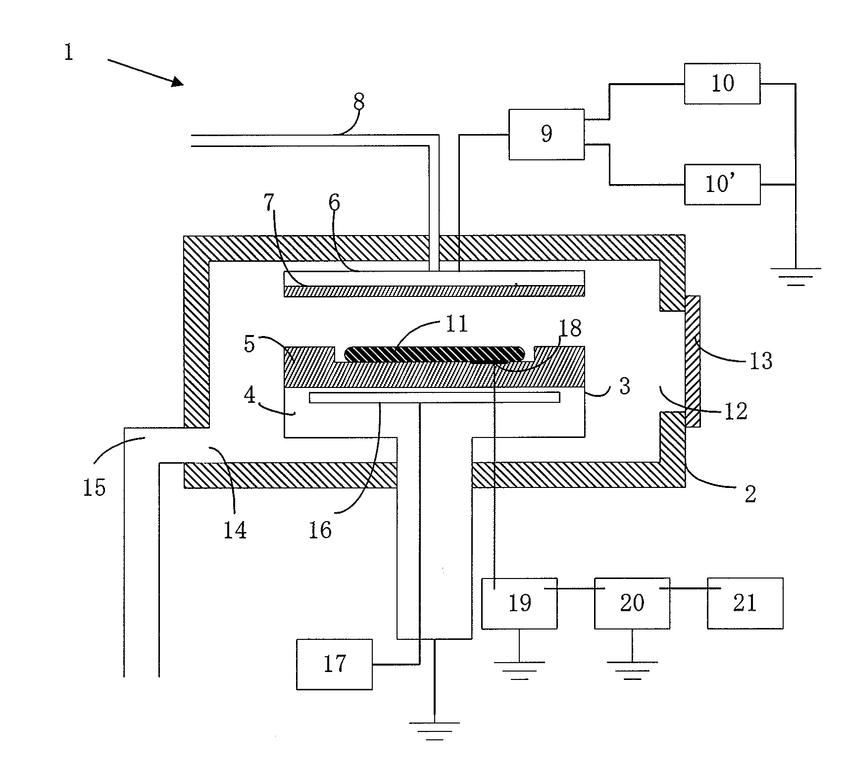
[0055]Numeral 18 in FIG. 1 indicates a measurement electrode that contacts the substrate 11 and measures the substrate voltage. The signal from the measurement electrode is connected to a static field strength meter 20 outside the reactor 2 via a RF removal filter 19, and the static strength meter 20 measures the DC bias voltage of the substrate 11. Any RF removal filter can be used as long as it can remove radio frequencies. Normally, this filter can be constituted by combining a coil, resistor and capacitor. The static field strength meter, which is also called a surface potential meter, may be any device as long as it can measure the surface potential (or charge potential) of a charged object based on the static field strength of the object. For your information, although the static field strength of the measuring target is measured without contacting the target, in this figure the potential of the substrate is sent to the static field strength meter throug...
example 2
(Tunnel Top Plate)
[0059]An example of a susceptor used to measure the substrate voltage is shown in FIGS. 3(a) and 3(b). A top plate 31 is detachably / attachably affixed to the susceptor with screws, etc. The top plate 31 is made of aluminum, aluminum alloy, etc., and its top and side faces are treated by anodic oxidation.
[0060]The top plate 31 has a hole 39 with a diameter of approx. 1 cm, and a single groove 38 connecting this hole to the periphery is provided on the reverse side. A measurement electrode 37 for measuring the substrate voltage and an electrode cover 34 made of an insulating material are inserted into this hole 39. The measurement electrode is typically made of aluminum, but nickel, tungsten, stainless steel or any other conductive material can be used without specific limitations. The insulating material is normally ceramic or quartz but is not limited thereto and it may be made of at least one material constituted by an oxide, nitride, or fluoride of aluminum, magn...
example 3
(Top Plate, Heater-Through Type)
[0065]Another example of a susceptor for measuring the substrate voltage is shown in FIGS. 4(a) and 4(b). Although the susceptor shown in this example is a separate type, either an integrated or separate susceptor may be used. A measurement electrode 47 pierces through a top plate 41 and connects to a conductive wire 43 via a heater 61. The measurement electrode 47 is encased in an insulation cylinder 44 to prevent the top plate 41 and heater 61 from contacting the electrode. The conductive wire 43 is covered with an insulating material 42 and guided to outside the reactor from the bottom of the heater along with other wires (such as a wire 63 connected to a heating element 62). The material of each part and other elements of configuration can be implemented according to Example 2. Here, the measurement electrode is positioned at the corresponding top plate surface (near the substrate center) in the axial direction as viewed from the bottom face of th...
PUM
| Property | Measurement | Unit |
|---|---|---|
| Electrical resistance | aaaaa | aaaaa |
| Strength | aaaaa | aaaaa |
Abstract
Description
Claims
Application Information