Nonvolatile semiconductor memory element and manufacturing method thereof

a semiconductor memory element and non-volatile technology, applied in the direction of semiconductor devices, electrical devices, transistors, etc., can solve the problems of limited tunnel insulating layer formation, limited thin film formation, and difficult miniaturization

Inactive Publication Date: 2009-03-05
KK TOSHIBA
View PDF5 Cites 21 Cited by
  • Summary
  • Abstract
  • Description
  • Claims
  • Application Information

AI Technical Summary

Problems solved by technology

However, since forming the tunnel insulating film into a thin film degrades the charge retention characteristic, there is a limit to forming the tunnel insulating layer into a thin film.
However, in item (1), there is a limit to thin-film formation, taking into account the degradation of the charge retention characteristic of the charge storage layer.
In item (2), the top face and side face of the charge storage layer have to be covered with the block insulating layer, which makes the miniaturization difficult.
In that case, the reaction of the block insulating layer with the control gate electrode and charge storage layer arranged on and under the block insulating layer respectively is a problem.
For example, in a case where polysilicon is used for the charge storage layer and hafnium oxide is used for the block insulating layer, when the heat treatment is performed as described above, a low-dielectric oxidative reaction layer is formed between the polysilicon and the hafnium oxide, causing a problem: the interface structure changes its nature.
Consequently, the characteristics of the charge storage layer, block insulating layer, and control gate electrode deteriorate as a result of a decrease in the capacitance due to the series capacitance of the block insulating layer and the oxidative reaction layer or an increase in the leakage current caused by the modulation of the work function of the upper and lower electrodes.
Eventually, the characteristics of the memory cell transistor deteriorate.

Method used


Image

  • Nonvolatile semiconductor memory element and manufacturing method thereof
  • Nonvolatile semiconductor memory element and manufacturing method thereof
  • Nonvolatile semiconductor memory element and manufacturing method thereof

Examples


first embodiment

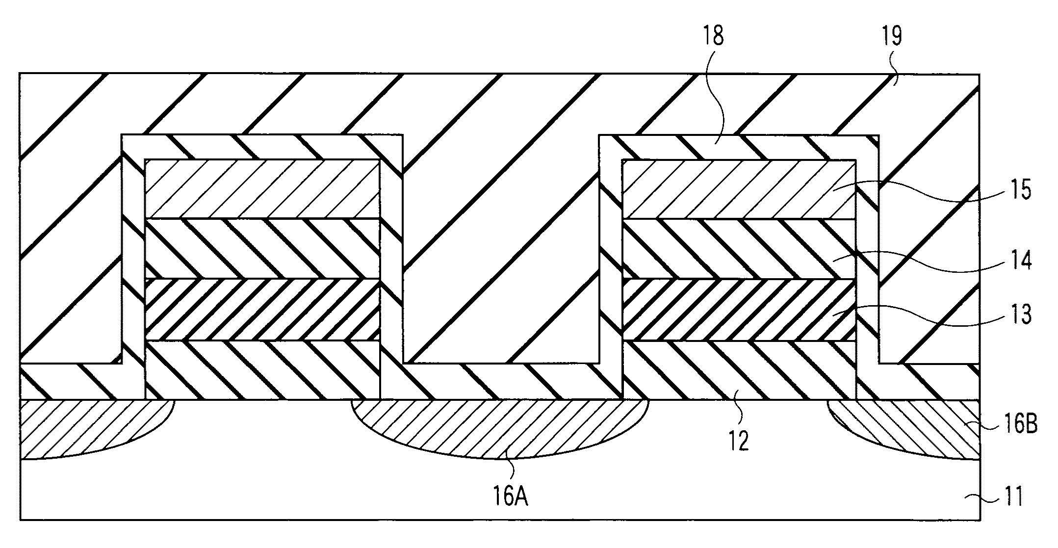
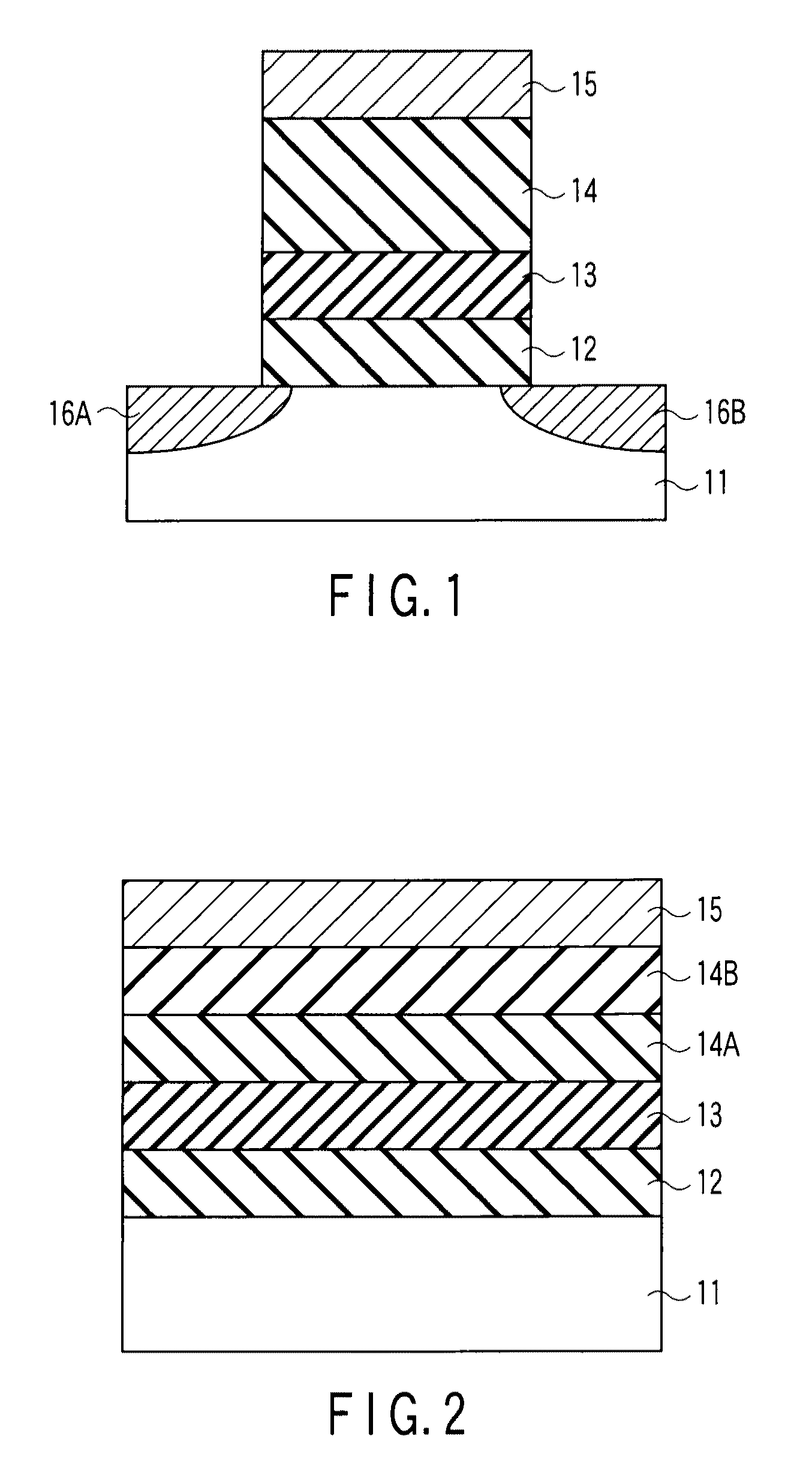
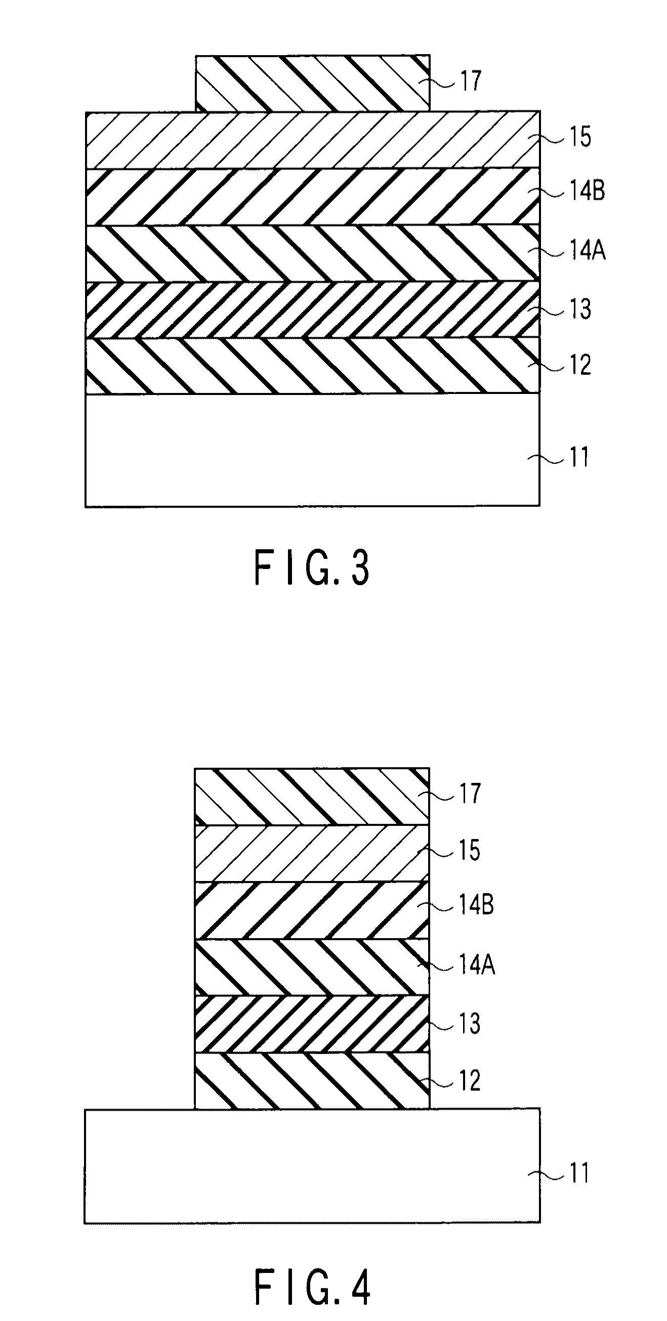
[0037]FIG. 1 is a sectional view illustrating a memory cell transistor (a nonvolatile semiconductor memory element) according to the first embodiment.

[0038]A p-type-conductivity substrate 11 is, for example, a p-type semiconductor substrate, a semiconductor substrate with a p-well, or an SOI (Silicon On Insulator) substrate with a p-type semiconductor layer. A semiconductor made of silicon (Si) or the like, or a compound semiconductor made of SiGe, GaAs, ZnSe, or the like is used as the semiconductor substrate 11.

[0039]In the semiconductor substrate 11, a source region 16A and a drain region 16B are provided separately. Each of the source region 16A and drain region 16B is composed of an n+-type diffused region formed by introducing highly-concentrated n+-type impurities (such as phosphorus (P) or arsenic (As)) into silicon.

[0040]On the semiconductor substrate 11 between the source region 16A and drain region 16B (that is, on the channel region), there is provided a gate structure i...

second embodiment

[0069]The second embodiment suppresses the reaction of the charge storage layer with the lanthanum aluminate layer more by inserting stabilized aluminum oxide between the charge storage layer and the lanthanum aluminate layer as a part of the block insulating layer. FIG. 9 is a sectional view illustrating a memory cell transistor according to the second embodiment.

[0070]In a semiconductor substrate 11, a source region 16A and a drain region 16B are provided separately. On the semiconductor substrate 11 between the source region 16A and drain region 16B (that is, on the channel region), there is provided a gate structure in which a tunnel insulating layer 12, a charge storage layer 13, a block insulating layer 14, and a control gate 15 are stacked one on top of another in that order.

[0071]The block insulating layer 14 has a stacked structure in which an aluminum oxide layer 14A and a lanthanum aluminate layer 14B are stacked one on top of the other in that order. The lanthanum alumin...

third embodiment

[0086]The third embodiment suppresses the reaction of the charge storage layer with the lanthanum aluminate layer more by inserting stabilized aluminum oxide between the charge storage layer and a lanthanum aluminate layer as a part of the block insulating layer. Moreover, the third embodiment suppresses the reaction of the control gate electrode with the lanthanum aluminate layer more by the insertion of stabilized aluminum oxide between the control gate electrode and the lanthanum aluminate layer. FIG. 16 is a sectional view illustrating a memory cell transistor according to the third embodiment.

[0087]In a semiconductor substrate 11, a source region 16A and a drain region 16B are provided separately. On the semiconductor substrate 11 between the source region 16A and drain region 16B (that is, on the channel region), there is provided a gate structure in which a tunnel insulating layer 12, a charge storage layer 13, a block insulating layer 14, and a control gate 15 are stacked on...


PUM


Abstract

A nonvolatile semiconductor memory element includes a semiconductor substrate, a source region and a drain region which are provided separately in the semiconductor substrate, a tunnel insulating layer which is provided between the source region and the drain region on the semiconductor substrate, a charge storage layer which is provided on the tunnel insulating layer, a block insulating layer which is provided on the charge storage layer and includes a crystallized lanthanum aluminate layer, and a control gate electrode which is provided on the block insulating layer.

Description

CROSS-REFERENCE TO RELATED APPLICATIONS[0001]This application is based upon and claims the benefit of priority from prior Japanese Patent Application No. 2007-222690, filed Aug. 29, 2007, the entire contents of which are incorporated herein by reference.BACKGROUND OF THE INVENTION[0002]1. Field of the Invention[0003]The present invention relates to a nonvolatile semiconductor memory element and a manufacturing method thereof, and, for example, to a nonvolatile semiconductor memory element which stores information by injecting or releasing a charge into or from a charge storage layer.[0004]2. Description of the Related Art[0005]A memory cell transistor in a flash memory or a MONOS (Metal Oxide Nitride Oxide Semiconductor) nonvolatile semiconductor memory device has a gate structure in which a tunnel insulating layer, a charge storage layer, a block insulating layer, and a control gate electrode are stacked on a semiconductor substrate. Data is written to or erased from the memory cel...

Claims


Application Information

Patent Timeline
Patent Type & Authority Applications(United States)
IPC IPC(8): H01L29/00
CPCH01L21/28273H01L21/28282H01L29/42324H01L29/792H01L29/517H01L29/7881H01L29/4234H01L29/40114H01L29/40117H10B63/30
Inventor TAKASHIMA, AKIRAKIKUCHI, SHOKOMURAOKA, KOICHI
Owner KK TOSHIBA
Why Eureka
Try Eureka