Light-emitting device

a technology of light-emitting diodes and diodes, which is applied in the direction of discharge tubes/lamp details, discharge tubes luminescnet screens, electric discharge lamps, etc., can solve the problems of yellow fluorescent substances that are defective in color rendering, poor white color to be emitted therefrom, and difficulty in applying yellow fluorescent substances for ordinary illumination or as backlights for liquid crystal displays

Active Publication Date: 2009-03-05
SAMSUNG ELECTRONICS CO LTD
View PDF13 Cites 72 Cited by
  • Summary
  • Abstract
  • Description
  • Claims
  • Application Information

AI Technical Summary

Benefits of technology

[0017]a first transparent resin layer covering the semiconductor light-emitting element and contacted with the first portion and the second portion, the first transparent resin layer having an arch-like outer profile, as seen in a cross section when cut perpendicularly to the surface; and
[0018]a laminated body formed on the first transparent resin layer with end faces of the laminated body being contacted with the second portion, the laminated body having an arch-like outer profile, as seen in a cross section when cut perpendicularly to the surface and comprising a red fluorescent layer, a yellow fluorescent layer, a second transparent resin layer, a green fluorescent layer and a blue fluorescent layer which are laminated in the mentioned order, the second transparent resin layer having a top portion larger in thickness than that of the end face portions thereof.

Problems solved by technology

Although this white LED is simple in construction, the white color to be emitted therefrom is poor in a red component.
Because of this, the white light obtained from a combination consisting of only the blue emission to be derived from an excitation light source and the yellow fluorescent substance has been realized as being defective in that it lacks in color rendering.
Therefore, this white light is accompanied with a problem that it is difficult to apply it for ordinary illumination or as a backlight for a liquid crystal display where high color rendering is demanded.
When several kinds of fluorescent substances are employed, there is the possibility that fluorescence may be re-absorbed.

Method used


Image

  • Light-emitting device
  • Light-emitting device
  • Light-emitting device

Examples


example 1

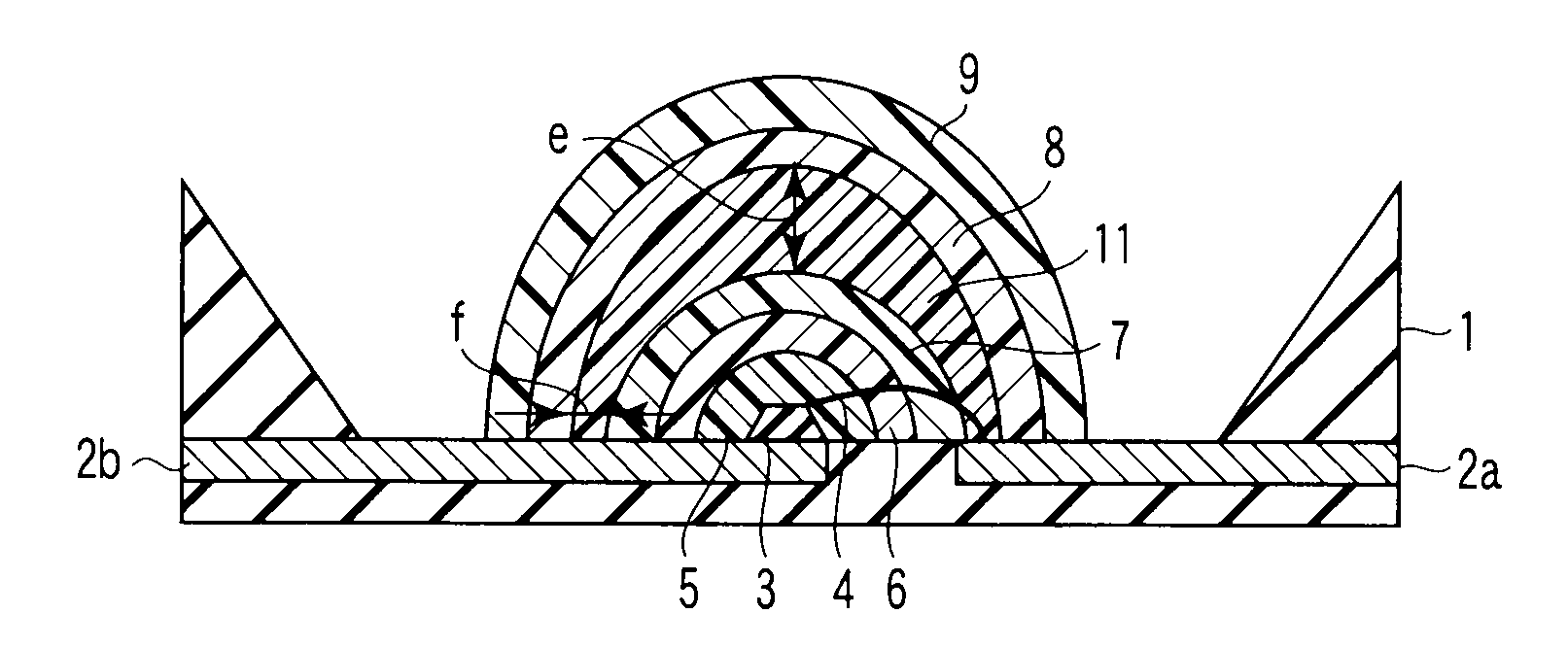
[0062]In this example, a light-emitting device constructed as shown in FIG. 2 was manufactured.

[0063]An ultraviolet LED chip exhibiting an emission peak at a wavelength ranging from 400 to 405 nm and having an InGaN-based compound semiconductor as an active layer and suitable p / n electrodes was prepared as a semiconductor light-emitting element 3. This semiconductor light-emitting element 3 was then secured to a package portion 1 by an Au—Sn paste. This package portion 1 was provided with lead-out electrodes 2a and 2b and with an aluminum nitride-based substrate having a wiring portion surrounded by a high reflectance material. The lead-out electrode 2a of the anode side was electrically connected with the p-type electrode of the ultraviolet LED chip by an Au wire 4. The lead-out electrode 2b of the cathode side was electrically connected with the n-type electrode of the ultraviolet LED chip by Au—Sn paste.

[0064]Using a silicone-based transparent resin, a transparent resin layer 5 w...

example 2

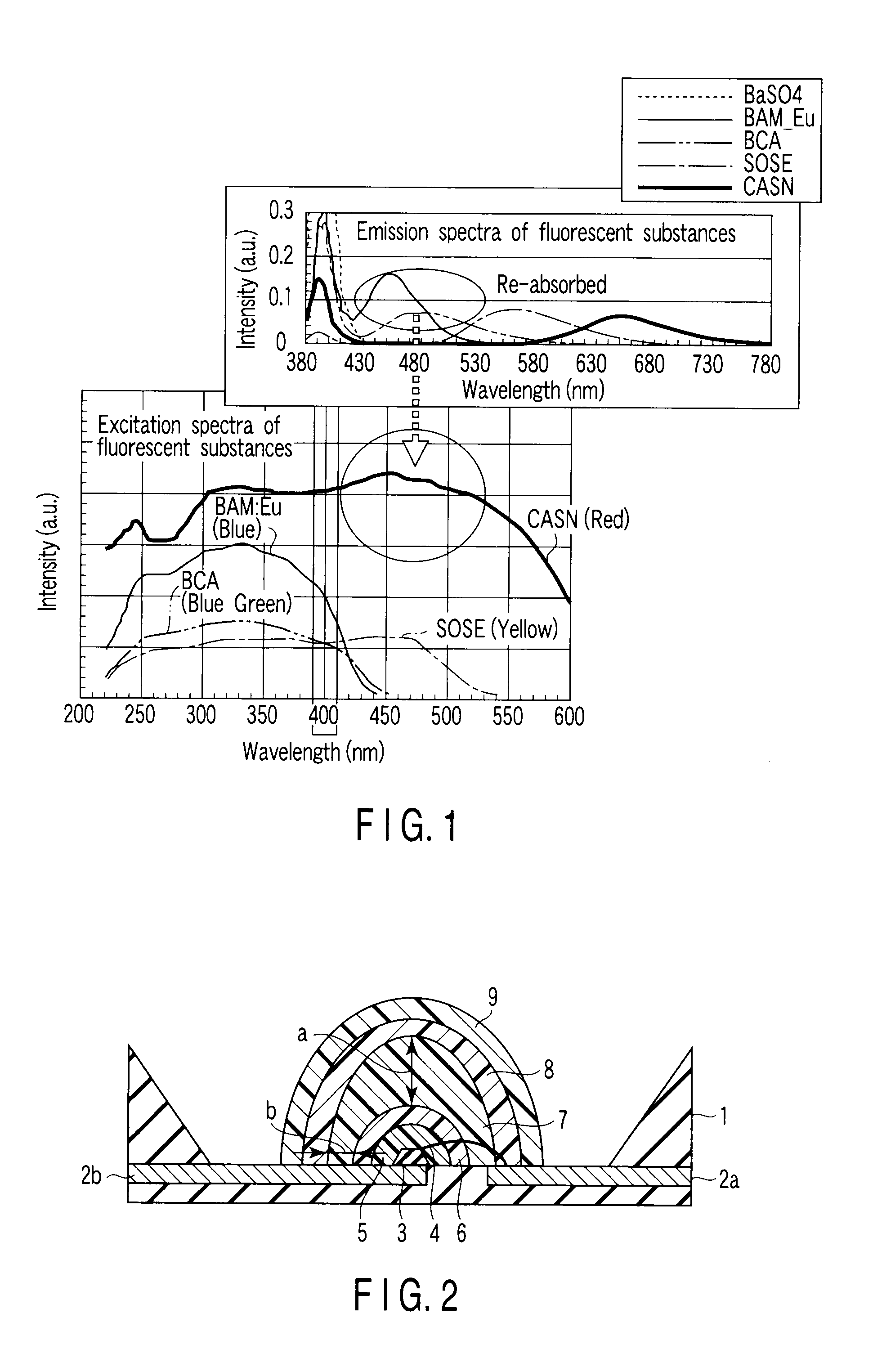
[0080]In this example, a light-emitting device constructed as shown in FIG. 3 was manufactured. By repeating the same procedures as described in Example 1, a transparent resin layer 5 and a red fluorescent layer 6 were formed on the same kind of semiconductor light-emitting element 3 as employed in Example 1.

[0081]An SOSE yellow fluorescent substance exhibiting an emission peak at a wavelength of 552 nm was dispersed in silicone resin to prepare a yellow fluorescent substance-dispersed resin. This yellow fluorescent substance-dispersed resin was laminated so as to entirely cover the red fluorescent layer 6 and to form a layer of an arch-like configuration having a uniform thickness, thereby forming a yellow fluorescent layer 7. Then, a second transparent resin layer 11 was formed on the yellow fluorescent layer 7 in such a manner that the thickness “e” of the top portion thereof was made larger than the thickness “f” of each of end faces thereof (i.e. e / f=2).

[0082]Further, a silicon...

example 3

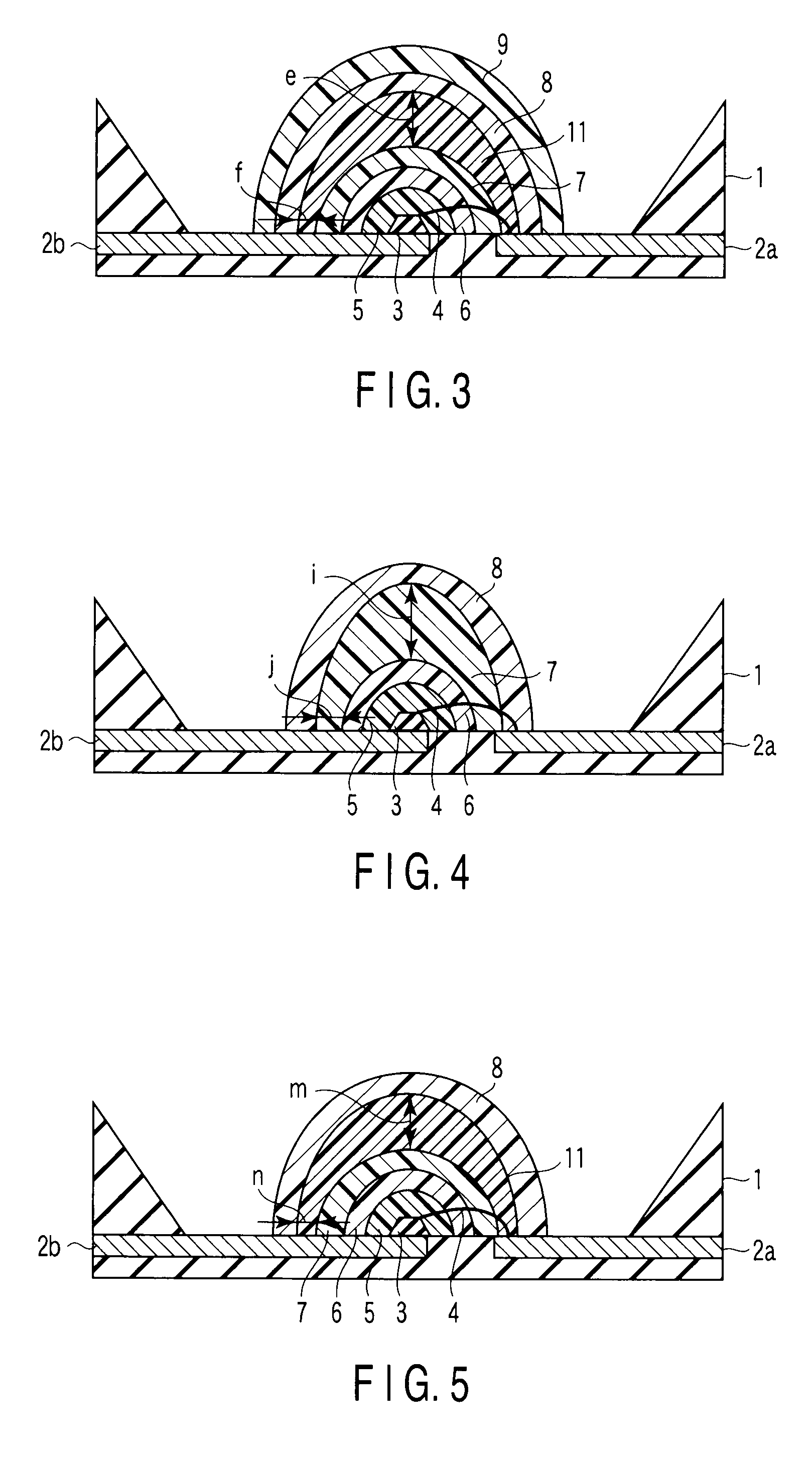
[0089]In this example, a light-emitting device constructed as shown in FIG. 4 was manufactured.

[0090]A blue LED chip exhibiting an emission peak at a wavelength ranging from 450 to 470 nm and having an InGaN-based compound semiconductor as an active layer and suitable p / n electrodes was prepared as a semiconductor light-emitting element 3. This semiconductor light-emitting element 3 was then secured to a package portion 1 by an Au—Sn paste. This package portion 1 was provided with lead-out electrodes 2a and 2b and with an aluminum nitride-based substrate having a wiring portion surrounded by a high reflectance material. The lead-out electrode 2a of the anode side was electrically connected with the p-type electrode of the blue LED chip by an Au wire 4. The lead-out electrode 2b of the cathode side was electrically connected with the n-type electrode of the blue LED chip by Au—Sn paste.

[0091]Using a silicone-based transparent resin, a transparent resin layer 5 was formed on the semic...


PUM


Abstract

A light-emitting device is provided, which includes a package having a first portion and a second portion surrounding it, a semiconductor light-emitting element mounted on the first portion and emitting a light having an emission peak in a near-ultraviolet region, a transparent resin layer covering the semiconductor light-emitting element and contacted with the package, and a laminated body formed on the transparent resin layer with end faces of the laminated body being contacted with the second portion. The transparent resin layer has an arch-like outer profile perpendicular cross section. The laminated body has an arch-like outer profile in perpendicular cross section and comprises a red fluorescent layer, a yellow fluorescent layer, a green fluorescent layer and a blue fluorescent layer laminated in the mentioned order. The yellow fluorescent layer has a top portion which is made larger in thickness than that of the end face portions thereof.

Description

CROSS-REFERENCE TO RELATED APPLICATIONS[0001]This application is based upon and claims the benefit of priority from prior Japanese Patent Application No. 2007-225887, filed Aug. 31, 2007, the entire contents of which are incorporated herein by reference.BACKGROUND OF THE INVENTION[0002]1. Field of the Invention[0003]This invention relates to a light-emitting diode (hereinafter referred to as LED) and a light-emitting device employing a semiconductor light-emitting element such as a semiconductor laser diode (hereinafter referred to as LD).[0004]2. Description of the Related Art[0005]In recent years, much attention has been paid to so-called white LEDs, where white light is emitted using a single chip comprising a combination of a blue LED employed as an excitation light source and a yellow fluorescent substance such as YAG:Ce. Although this white LED is simple in construction, the white color to be emitted therefrom is poor in a red component. Because of this, the white light obtain...

Claims


Application Information

Patent Timeline
Patent Type & Authority Applications(United States)
IPC IPC(8): H01J1/62H01L33/32H01L33/50H01L33/54H01L33/56H01L33/62
CPCH01L33/504H01L2224/45144H01L2224/48247H01L2924/00
Inventor MITSUISHI, IWAONUNOUE, SHINYAHATTORI, YASUSHI
Owner SAMSUNG ELECTRONICS CO LTD
Why Eureka
Try Eureka