Semiconductor device manufacturing method using double patterning and mask

a manufacturing method and mask technology, applied in the direction of microlithography exposure apparatus, instruments, photomechanical treatment, etc., can solve the problems of unconsidered improvement of yield in each process, undesirable reducing yield, etc., and achieve the effect of avoiding yield reducing factors

Inactive Publication Date: 2009-03-05
RENESAS ELECTRONICS CORP
View PDF5 Cites 27 Cited by
  • Summary
  • Abstract
  • Description
  • Claims
  • Application Information

AI Technical Summary

Benefits of technology

[0007]The present invention has been made in view of the foregoing problems, and one object thereof is to provide a semiconductor device manufacturing method in which layout patterns are distributed so as to avoid yield reducing factors, and a mask for use therein.
[0008]Another object of the present invention is to provide a semiconductor device manufacturing method that leverages flexibility obtained by distributing layout patterns to a plurality of masks thereby realizing improved yield, and a mask for use therein.
[0010]According to the embodiment, a group of layout patterns can be distributed to a plurality of masks so as to obtain layout patterns with which manufacturing is more facilitated in exposure steps, and so as to exclude layout patterns with which manufacturing is difficult. Thus, manufacturing is facilitated and yield is improved.

Problems solved by technology

However, the conventional technique sometimes distributes layout patterns that actually should not be distributed, thereby undesirably reducing yield.
Furthermore, it has not been considered to improve yield in each process after distribution, by the manner of distribution.

Method used


Image

  • Semiconductor device manufacturing method using double patterning and mask
  • Semiconductor device manufacturing method using double patterning and mask
  • Semiconductor device manufacturing method using double patterning and mask

Examples


first embodiment

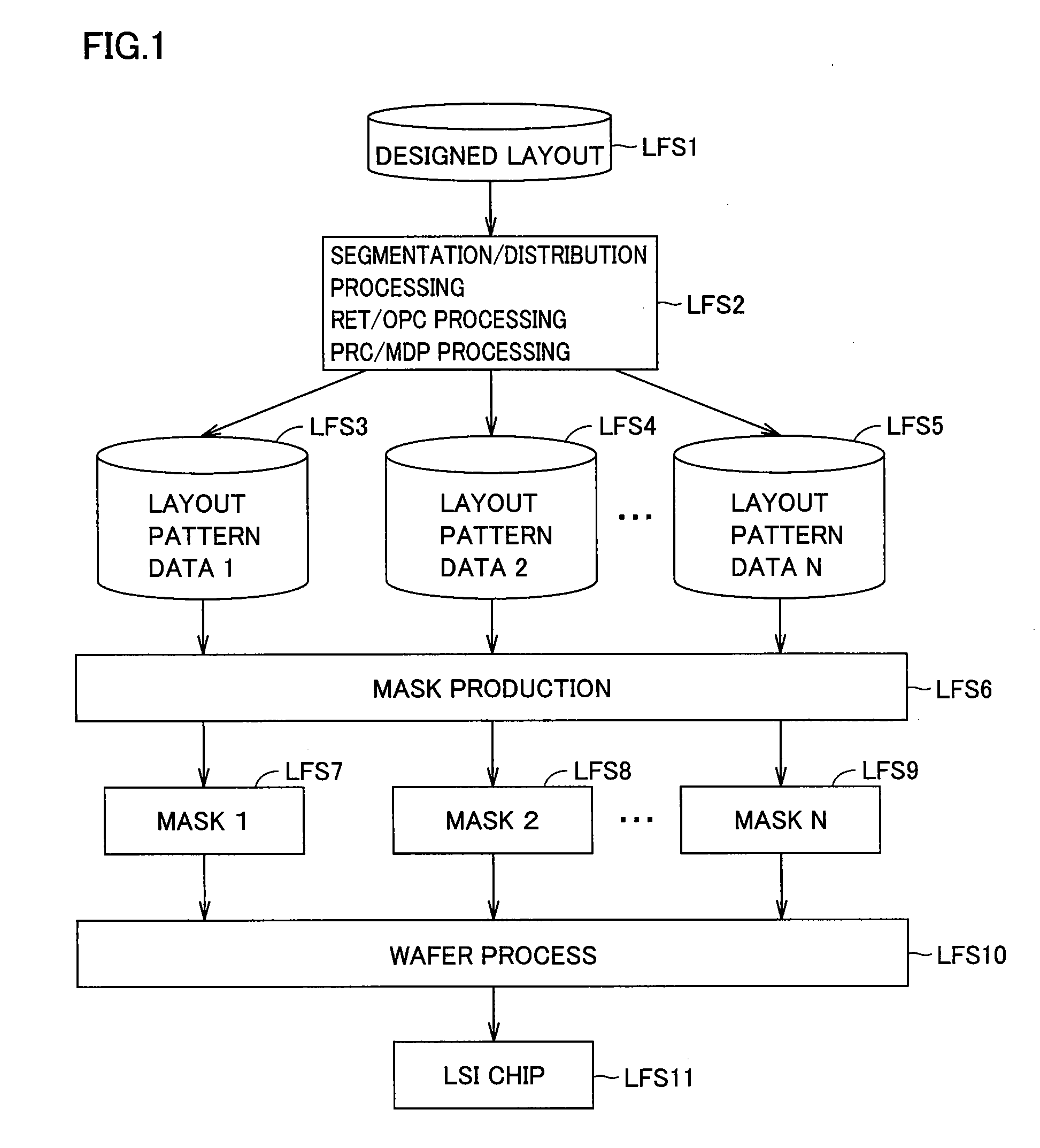
[0037]FIG. 1 shows a semiconductor device manufacturing method using double patterning. As shown in FIG. 1, in an LSI manufacturing flow of the present embodiment, firstly an intended designed layout is determined (LFS1). Next, in step (LFS2), segmentation / distribution processing, RET (Resolution Enhancement Technique), OPC (Optical Proximity Correction) processing, PRC (Process Rule Check), MDP (Mask Data Preparation) processing and the like are provided to the designed layout. Thus, layout pattern data 1, 2 . . . N is obtained (LFS 3-5). It should be noted that, as used herein, the optical proximity correction refers not only to optical proximity effect, but also to various pattern distortions in manufacturing. PRC refers to detection of problems in manufacturing, such as lithography verification that detects problems in a lithography process, MRC (Mask Rule Check) that detects problems in a mask process, and check for conditions that must be satisfied in imaging.

[0038]Next, in st...

second embodiment

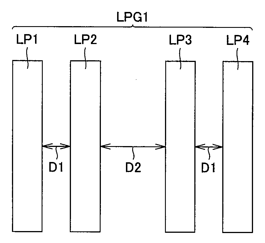
[0068]In the present embodiment, description will be given as to another example of distributing designed layout pattern to a plurality of masks that is performed in segmentation / distribution condition determining step (SDS8) shown in FIG. 4. This is an example being different from the first embodiment, in which originally separated designed layout patterns are distributed to a plurality of masks. Here, a designed layout pattern that is not originally separated is segmented into a plurality of layout patterns, and thereafter distributed to a plurality of masks. Also herein, layout patterns are distinguishably allotted to the masks. FIG. 9A shows a layout pattern group LPG2 that is the designed layout pattern. FIGS. 9B and 9C are schematic views showing examples where layout pattern group LPG2 is segmented at the identical location to obtain layout patterns LP11 and LP12.

[0069]In FIG. 9B, out of the segmented layout patterns LP11 and LP12, layout pattern LP11 that is relatively great...

third embodiment

[0072]In the present embodiment, description will be given as to an example where a subsidiary pattern is formed in a mask in addition to the layout patterns in segmentation / distribution condition determining step (SDS8) shown in FIG. 4. A subsidiary pattern refers to a pattern added to original designed layout patterns in order to obtain a pattern pitch or a pattern density that is desirable in manufacturing. Addition of the subsidiary pattern achieves the effect such as improved resolution or increased depth of focus, whereby the pattern shape can be improved.

[0073]FIG. 10A shows a layout pattern LP21 as a designed layout pattern. FIG. 10B shows a pattern AP21 that is actually obtained on a wafer for layout pattern LP21 in FIG. 10A.

[0074]FIG. 10C shows an example where a subsidiary pattern SP22 is added to FIG. 10A. When broadly classified, the subsidiary pattern includes a non-resolving subsidiary pattern with which only the pattern such as pattern AP21 shown in FIG. 10B is obtai...


PUM

PropertyMeasurementUnit
sizeaaaaaaaaaa
sizeaaaaaaaaaa
sizeaaaaaaaaaa

Abstract

To provide a semiconductor device manufacturing method using double patterning, in which layout patterns are distributed avoiding yield reduction factors. The semiconductor device manufacturing method includes the steps of: preparing a plurality of masks for use in the double patterning; and performing the double patterning using the plurality of masks. The step of preparing the plurality of masks includes a step of distributing a group of layout patterns to the plurality of masks, in accordance with characteristics of exposure steps respectively using the plurality of masks, and in consideration of size of the layout patterns.

Description

BACKGROUND OF THE INVENTION[0001]1. Field of the Invention[0002]The present invention relates to a semiconductor device manufacturing method and a mask, and in particular, to a manufacturing method of a semiconductor device having a fine semiconductor circuit pattern and a mask for use in manufacturing the same.[0003]2. Description of the Background Art[0004]As a promising candidate for lithography technique of 32 nm node, double patterning has been proposed. Double patterning is a process for obtaining designed layout patterns, by distributing layout patterns into a plurality of masks and performing a plurality of exposure processes, etching processes and the like. When the distance between two layout patterns is small, if the two layout patterns are formed on an identical mask, the two layout patterns cannot separately be formed on a wafer. Double patterning is used to avoid such a problem.[0005]The layout pattern distribution process is performed as follows, for example. Specific...

Claims


Application Information

Patent Timeline
Patent Type & Authority Applications(United States)
IPC IPC(8): G03F7/20G03F1/36G03F1/68G03F1/70H01L21/027
CPCG03F1/144G03F7/70466G03F7/70283G03F1/70G03F1/36G03F7/70441
Inventor TAOKA, HIRONOBUMONIWA, AKEMISAKAI, JUNJIRO
Owner RENESAS ELECTRONICS CORP
Why Eureka
Try Eureka