Orientation-optimized pfets in CMOS devices employing dual stress liners

a technology of cmos and pfets, applied in the direction of semiconductor devices, basic electric elements, electrical equipment, etc., can solve the problems of affecting the performance of a particular semiconductor device, the scaling of semiconductor devices, etc., and achieve the effect of increasing the conductivity of an inversion layer

Inactive Publication Date: 2009-03-12
GLOBALFOUNDRIES INC
View PDF10 Cites 10 Cited by
  • Summary
  • Abstract
  • Description
  • Claims
  • Application Information

AI Technical Summary

Benefits of technology

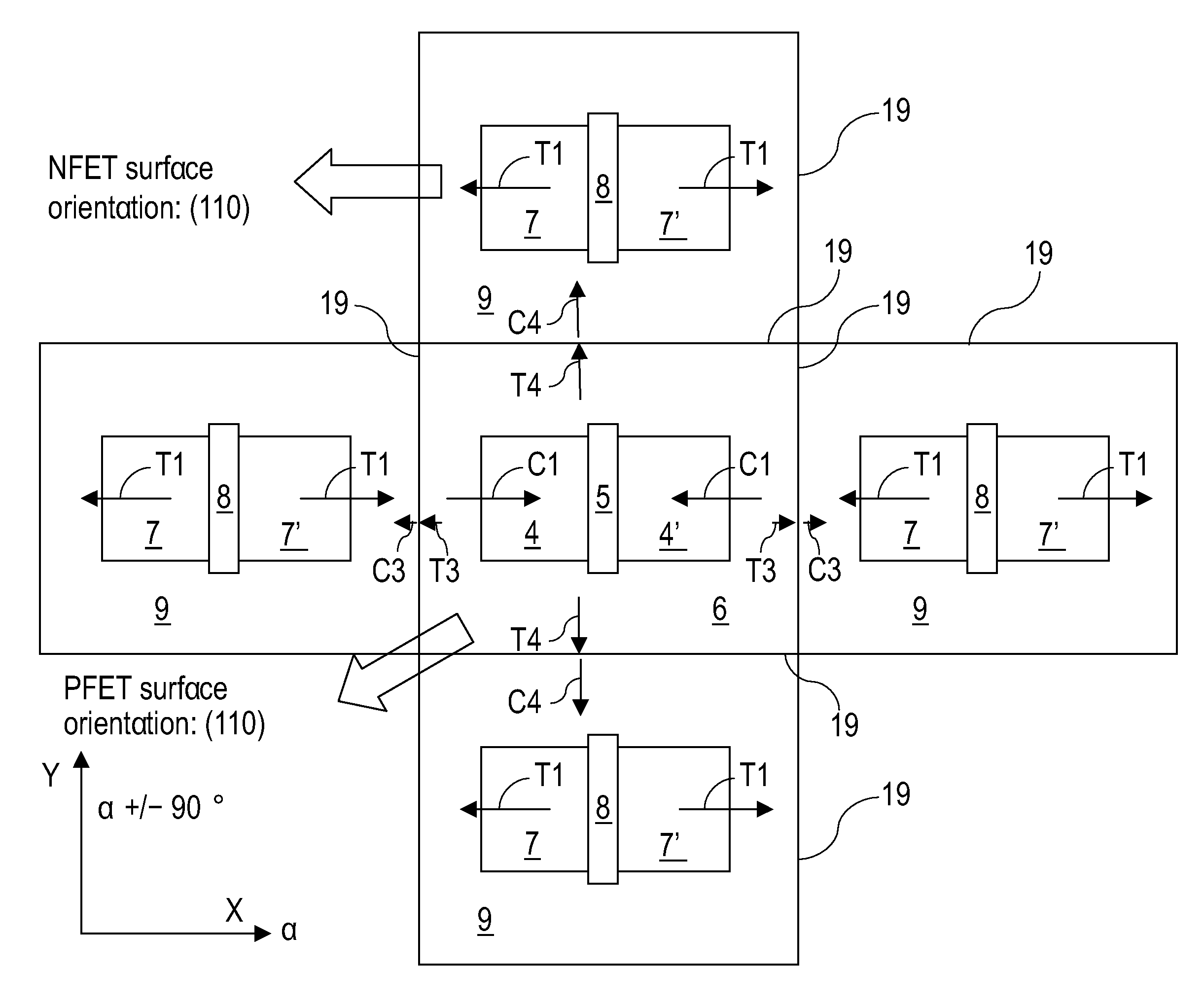
[0017]Secondary tensile stresses are most beneficial to neighboring PFETs when secondary longitudinal tensile stresses are minimized and secondary transverse tensile stresses are maximized. The effects of these secondary stresses generally increase as FET dimensions and PFET-to-NFET spacings shrink. Maximum advantage is thus obtained when longitudinally adjacent NFETs become further away from the PFET and when transversely adjacent NFETs become closer to the PFET, the latter situation naturally occurring as the long dimension of the PFET gate line (i.e., the one perpendicular to current flow) decreases. Typically, center-to-center spacings of adjacent PFETs and NFETs for the devices of this invention would be in the range 0.5 to 3 μm, with the most typical spacings averaging around 1 μm.
[0018]In the present invention, the physical directions of the gate line of the PFET and the gate line of the at least one NFET are the same. Longitudinal tensile channel strain in the at least one NFET typically increases the conductivity of an inversion layer of the at least one NFET. The at least one NFET may be formed on the same (110) silicon substrate, or preferably, formed on another silicon layer having a (001) surface orientation.

Problems solved by technology

As the device scale approaches nanometer ranges, further scaling of semiconductor devices faces various challenges.
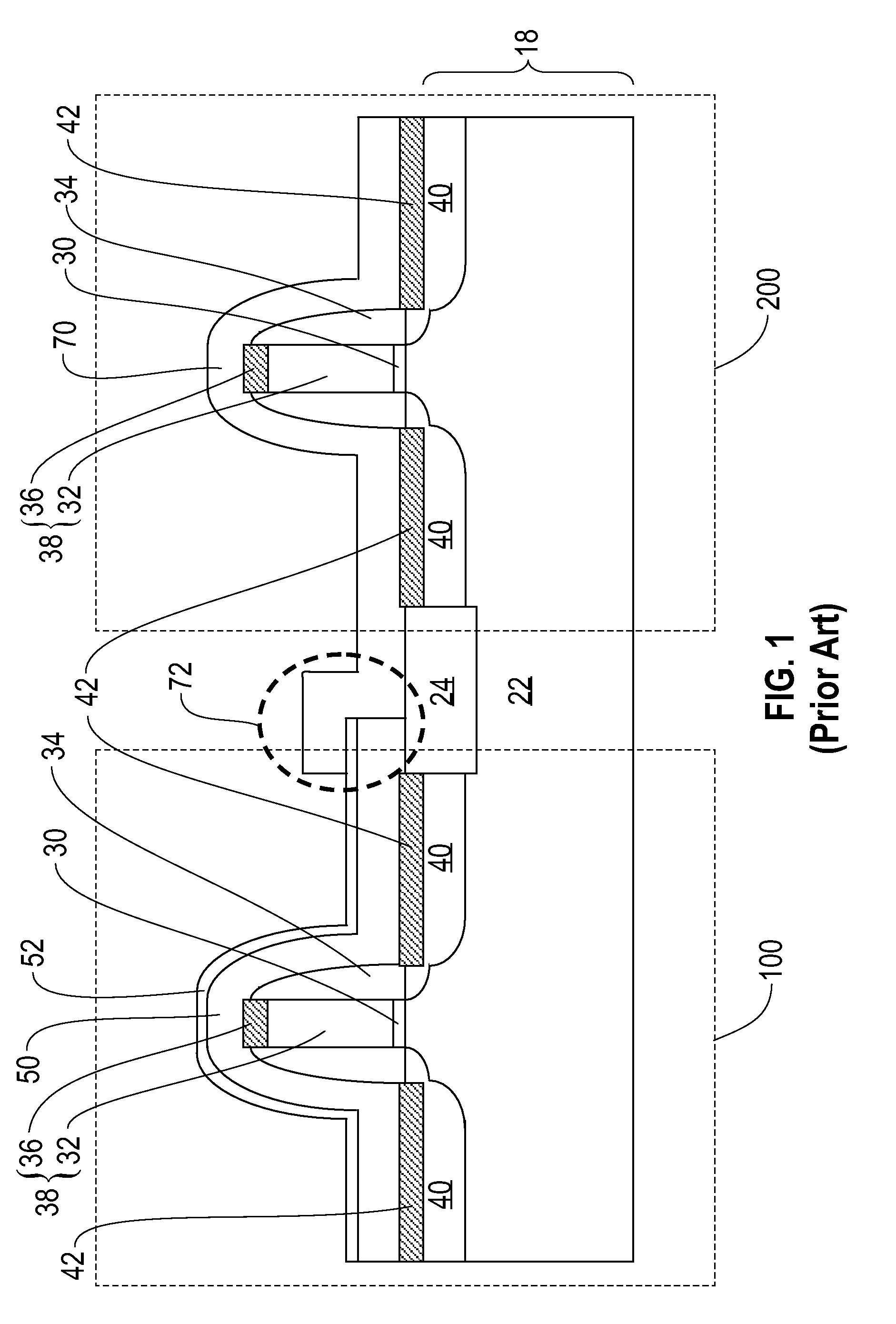
Further, when multiple stress-generating structures are formed on a semiconductor substrate, the performance of a particular semiconductor device is affected by primary stress effects from stress-generating structures in the particular semiconductor device itself, as well as by secondary stress effects from stress-generating structures in adjacent devices.

Method used


Image

  • Orientation-optimized pfets in CMOS devices employing dual stress liners
  • Orientation-optimized pfets in CMOS devices employing dual stress liners
  • Orientation-optimized pfets in CMOS devices employing dual stress liners

Examples


Embodiment Construction

[0064]As stated above, the present invention relates to complementary metal oxide semiconductor (CMOS) transistors with enhanced mobility through biaxial stress generated by dual stress liners, which are now described in detail with accompanying figures. It is noted that like and corresponding elements are referred to by like reference numerals.

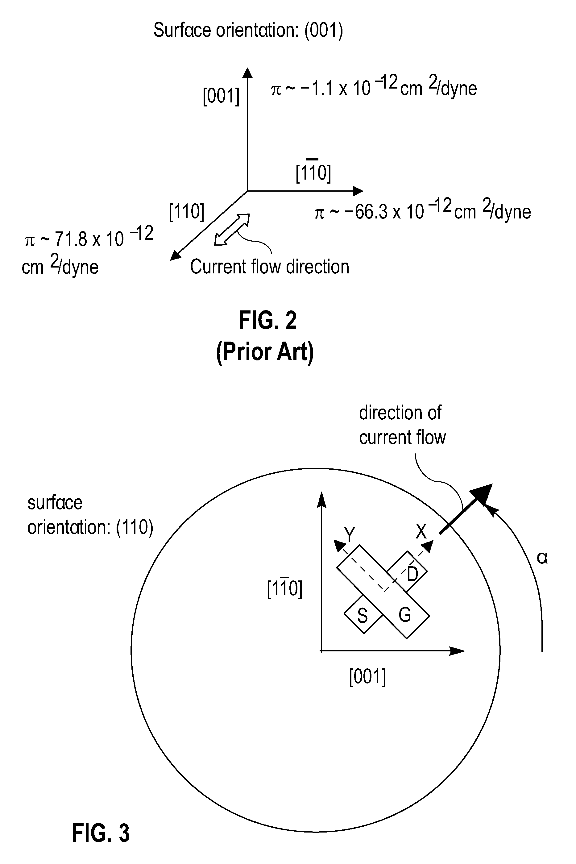
[0065]It is understood that due to inherent symmetry in the crystallographic structure of silicon, the (001) surface orientation may be considered a (100) surface orientation, a (010) surface orientation, a (00 1) surface orientation, etc. in alternate coordinate systems. Likewise, a (110) surface orientation may be considered an (1 10) orientation, etc. Such equivalency is implied herein even when not explicitly stated. Further, it is also understood that when different equivalent surface orientations or crystallographic directions are distinguished, for example, between a [110] crystallographic direction and a [1 10] crystallographic direct...


PUM


Abstract

A PFET is provided on a silicon layer having a (110) surface orientation and located in a substrate. A compressive stress liner disposed on the gate and source/drain regions of the PFET generates a primary longitudinal compressive strain along the direction of the PFET channel. A tensile stress liner disposed on at least one NFET located transversely adjacent to the PFET generates a primary longitudinal tensile strain along the direction of the NFET channel. A secondary stress field from the at least one NFET tensile liner generates a beneficial transverse tensile stress in the PFET channel. The net benefits of the primary compressive longitudinal strain and the secondary tensile transverse stress are maximized when the azimuthal angle between the direction of the PFET channel and an in-plane [1 10] crystallographic direction in the (110) silicon layer is from about 25° to about 55.

Description

FIELD OF THE INVENTION[0001]The present invention generally relates to semiconductor devices for integrated circuits, and particularly to orientation-optimized p-type field effect transistors (PFETs) in complementary metal oxide semiconductor (CMOS) transistors employing dual stress liners.BACKGROUND OF THE INVENTION[0002]Continuous scaling of silicon-based metal oxide semiconductor field effect transistors (MOSFETs) has contributed to relentless advances in semiconductor technology. As the device scale approaches nanometer ranges, further scaling of semiconductor devices faces various challenges. In light of this, many methods of improving device performance without resorting to scaling have recently been explored.[0003]One widely adopted approach for improving performance of semiconductor devices without relying on scaling is to increase carrier (electron or hole) mobility in a MOSFET. When stress is applied to the channel of a semiconductor transistor, the mobility of carriers, a...

Claims


Application Information

Patent Timeline
Patent Type & Authority Applications(United States)
IPC IPC(8): H01L27/12
CPCH01L21/823807H01L29/7843H01L29/045
Inventor YIN, HAIZHOUSAENGER, KATHERINE L.SUNG, CHUN-YUNGXIU, KAI
Owner GLOBALFOUNDRIES INC
Why Eureka
Try Eureka