Semiconductor device and manufacturing method of the same

a technology of semiconductor devices and manufacturing methods, applied in semiconductor devices, semiconductor/solid-state device details, electrical apparatus, etc., can solve the problems of inability to utilize aluminium which is generally employed as a material of element electrodes, complex assembling steps, and cost-up aspects, and achieve high thermal conductivity, simple assembling steps, and high electric conductivity

Inactive Publication Date: 2009-03-12
PANASONIC SEMICON SOLUTIONS CO LTD
View PDF6 Cites 7 Cited by
  • Summary
  • Abstract
  • Description
  • Claims
  • Application Information

AI Technical Summary

Benefits of technology

[0018]With employment of the above-described structure, even in such a case that the second conductor itself does not have a sufficiently strong strength, the strength of the second conductor can be compensated by the first conductor, so that stronger joining effect can be achieved. Also, the function capable of realizing the higher electric conductivity and the higher thermal conductivity, which are owned by the first conductor, and the function capable of simplifying the electric connection between the element electrode of the semiconductor element and the lead, which are owned by the second conductor, can be provided with respect to the coupling conductor.
[0027]As previously described, since plural pieces of the above-described coupling conductors are employed, both the element electrode and the lead may be electrically connected to these coupling conductors. As a consequence, the coupling conductors can be employed with respect to the element electrode and the lead, which have various sorts of dimensions, so that the cost thereof can be reduced. Also, as compared with such a case that a coupling conductor is formed in such a manner that a width of a single coupling conductor is made wider, since this wide coupling conductor is divided into a plurality of coupling conductors, the following merits may be achieved. That is, these divided coupling conductors can be readily handled; higher bonding characteristics thereof may be obtained; and even when these divided coupling conductors are bent, the bending resistivity thereof may be maintained.
[0029]As a consequence, even when solder, or the like is not employed, the coupling conductor can be connected to both the element electrode and the lead, so that the coupling conductor can be provided with higher electric conductivity and high thermal conductivity. Also, since the step for employing the solder is no longer required, the assembling step can be made simpler. In addition, since the coupling conductor is equipped with the concave / convex shape, the close adhesive characteristic can be increased without increasing the strength during the ultrasonic connecting operation.

Problems solved by technology

In order to reduce ON resistances, several tens to several hundreds of either gold wires or aluminium wires are necessarily employed, which may cause cost-up aspects, and assembling steps to become complex.
Also, in order that a metal material having a superior solder accepting characteristic must be employed as an element electrode, there is a problem that aluminium which is generally employed as a material of an element electrode cannot be utilized.
As a result, there is such a demerit that the thickness of the package of the semiconductor device becomes thicker.

Method used


Image

  • Semiconductor device and manufacturing method of the same
  • Semiconductor device and manufacturing method of the same
  • Semiconductor device and manufacturing method of the same

Examples


embodiment mode 1

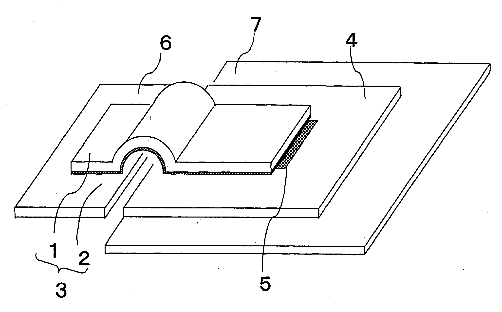
[0040]FIG. 1 is a perspective view for indicating a semiconductor device according to an embodiment mode 1 of the present invention. In FIG. 1, while a semiconductor element 4 has been electrically connected via a coupling conductor 3 to one end of a lead 6 of a lead frame, a first conductor 1 is a plate-shaped conductor that contains copper as a major component, and a second conductor 2 is an aluminium layer. The aluminium layer is employed in order to electrically connect an element electrode 5 formed on the semiconductor element 4 to the lead 6 of the lead frame. This coupling conductor 3 has been manufactured by stacking the second conductor 2 on one plane of the first conductor 1, and, in FIG. 1, has been formed in a layer shape in such a manner that the first conductor 1 may be electrically connected on the second conductor 2. Although a plane of the second conductor 2 provided on the side to be electrically connected to the lead 6 is plain, concave / convex portions may be alte...

embodiment mode 2

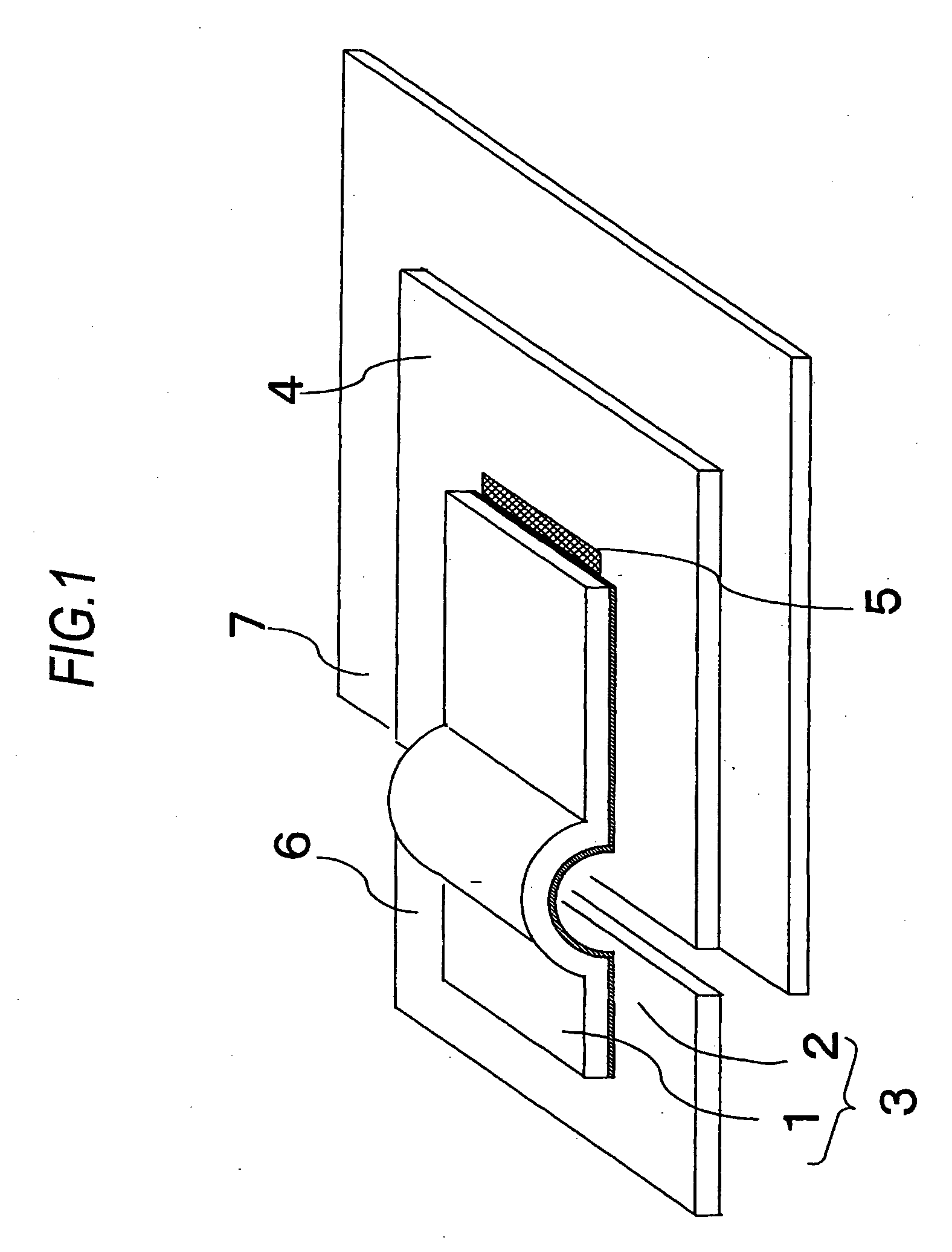
[0048]FIG. 2 is a schematic diagram of a semiconductor device according to an embodiment mode 2 of the present invention. A structural difference from that of the above-described embodiment mode 1 is given as follows: That is, a second conductor 2 constructed of an aluminium layer has been provided with respect only to such a region which is electrically connected to both an element electrode 5 and a lead 6 by performing an ultrasonic connecting method. It should be understood that in the below-mentioned embodiment mode 2, the same reference numerals will be employed as those for denoting the same structural elements explained in the embodiment mode 1, and detailed descriptions thereof will be omitted.

[0049]In accordance with the above-described structure, in addition to the operation effects achieved by the above-described embodiment mode 1, since a portion that becomes a curved shape is a layer structure of a first conductor 1, a mechanical strength can be maintained, while stripp...

embodiment mode 3

[0053]FIG. 3 is a schematic diagram of a coupling conductor that is employed in order to mount a semiconductor device according to an embodiment mode 3 of the present invention. It should be understood that in the below-mentioned embodiment mode 3, the same reference numerals will be employed as those for denoting the same structural elements explained in the embodiment mode 1, and detailed descriptions thereof will be omitted.

[0054]In FIG. 3, a second conductor 2 has been formed by such a conductor having a plate shape made of combining concaves / convexes, curved planes, and flat planes with each other. FIG. 4 is a plan view of the above-described second conductor 2, as viewed from the side for forming the second conductor 2. In this embodiment mode 3, more specifically, the plate-shaped conductor having the concave / convex shape is employed in such a region which the second conductor 2, the element electrode 5, and the lead 6 are electrically connected. As a result, a close adhesive...


PUM


Abstract

While a semiconductor device is provided with a plurality of element electrodes 5 formed on a semiconductor element 4 and a plurality of lead terminal electrodes 6 formed on a lead frame, the semiconductor device is equipped with a coupling conductor which electrically connects at least one electrode among the above-described element electrodes 5 to at least one electrode among the above-described lead terminal electrodes 6; the above-described coupling conductor is manufactured by a first conductor 1 and a second conductor 2, the major components of which are metals; the first conductor 1 has been electrically connected to the second conductor 2; and the element electrodes 5 and the lead terminal electrodes 6 have been electrically connected to the second electrode 2 respectively.

Description

BACKGROUND OF THE INVENTION[0001]1. Field of the Invention[0002]The present invention is related to a semiconductor device and a manufacturing method thereof. More specifically, the present invention is directed to a coupling conductor which connects a semiconductor element to a lead terminal, for instance, such a coupling conductor which electrically connects a source electrode of an MOSFET corresponding to one of semiconductor elements with a lead terminal thereof.[0003]2. Description of the Related Art[0004]Very recently, reductions of power consumption of semiconductor devices have been desired. As one of means for reducing the power consumption, various technical ideas capable of lowering ON resistances have been proposed, while the ON resistances correspond to essential resistance components of semiconductor devices when the semiconductor devices are operated. Among these technical ideas, a description is made of techniques capable of reducing ON resistances occupied by packag...

Claims


Application Information

Patent Timeline
Patent Type & Authority Applications(United States)
IPC IPC(8): H01L23/495H01L21/60
CPCH01L23/49524H01L24/31H01L2924/00014H01L2924/014H01L2924/01033H01L2924/01006H01L2924/13091H01L24/37H01L24/40H01L24/41H01L24/45H01L24/83H01L2224/45124H01L2224/45144H01L2224/83205H01L2224/83801H01L2924/01004H01L2924/01013H01L2924/01022H01L2924/01028H01L2924/01029H01L2924/01047H01L2924/01078H01L2924/01079H01L2924/01082H01L2224/48H01L2224/45015H01L2224/84205H01L24/84H01L2224/40091H01L2224/85345H01L2924/00H01L2224/73221
Inventor HAMADA, MITSUHIROTOMITA, KOUICHI
Owner PANASONIC SEMICON SOLUTIONS CO LTD
Why Eureka
Try Eureka