Encapsulated Organic Electronic Device With Improved Resistance To Degradation

a technology of organic electronic devices and encapsulated organic materials, applied in thermoelectric devices, discharge tubes/lamp details, discharge tubes luminescnet screens, etc., can solve the problems of rapid degradation of organic materials used in these devices, and the degradation of devices, so as to achieve the effect of improving strength and stability

Inactive Publication Date: 2009-03-12
STMICROELECTRONICS SRL
View PDF14 Cites 3 Cited by
  • Summary
  • Abstract
  • Description
  • Claims
  • Application Information

AI Technical Summary

Benefits of technology

[0009]The aim of embodiments of the present invention is consequently to provide processes, and devices formed by such processes, that will enable the afor

Problems solved by technology

However, the organic materials used in these devices undergo a rapid degradation in the presence of external agents such as light, oxygen and humidity (water vap

Method used


Image

  • Encapsulated Organic Electronic Device With Improved Resistance To Degradation
  • Encapsulated Organic Electronic Device With Improved Resistance To Degradation
  • Encapsulated Organic Electronic Device With Improved Resistance To Degradation

Examples


first embodiment

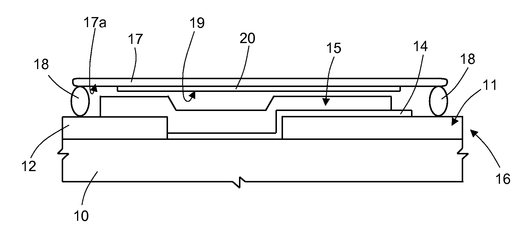
[0019]A manufacturing process according to the present invention is now described, envisaging the formation of an organic electronic device comprising a plurality of elementary components (in particular, bottom-emitting OLEDs) made at least in part of organic materials. In what follows, for reasons of simplicity of illustration, just two elementary components will be illustrated, but it should be clear that any number thereof may be formed.

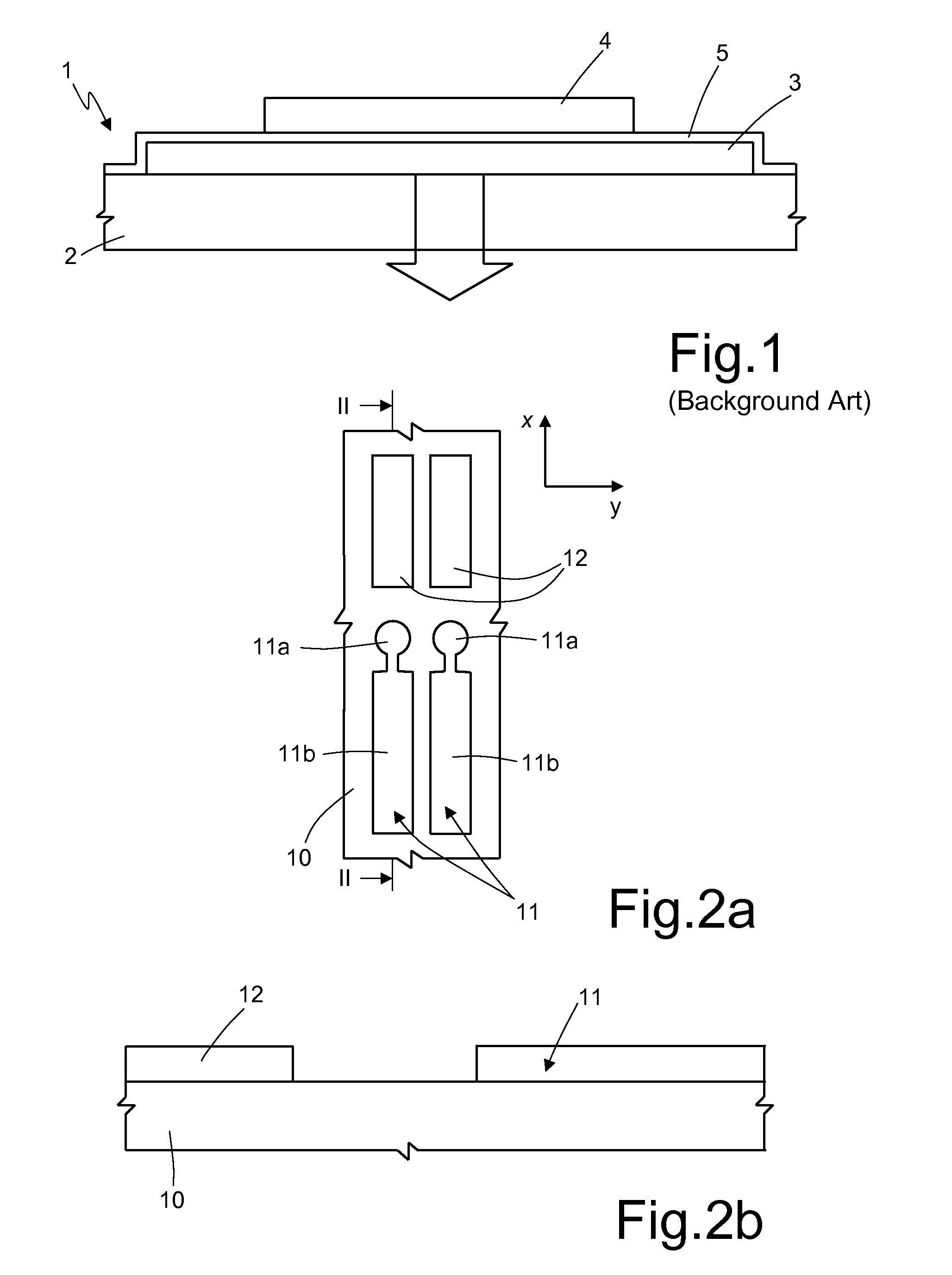
[0020]With reference to FIGS. 2a-2b (which are not drawn to scale, as neither are the subsequent figures), first electrodes (or anodes) 11 of the elementary components, and electrical contacts 12, are initially formed on a substrate 10 made of transparent material, for example, glass or plastic. As will be clarified, the electrical contacts 12 are designed to contact second electrodes of the elementary components so as to enable biasing thereof. A layer of transparent conductive material, for example ITO, is deposited on the substrate 10 and is th...

second embodiment

[0032]the present invention envisages the formation of an organic electronic device comprising elementary components 16 of a top-emitting OLED type.

[0033]In detail (FIG. 8), the electrical contacts 12, made for example of ITO, are initially deposited on the substrate 10, which here can be made of an opaque material. In this case, the electrical contacts 12 are designed to contact the first electrodes 11 to enable biasing thereof from outside the encapsulation.

[0034]Then (FIG. 9), the first electrodes 11, made for example of aluminium, are defined by means of a photolithographic process (or selective deposition / evaporation); the first electrodes 11 are set partially on respective electrical contacts 12 (contacting them), and extend partially on top of the substrate 10.

[0035]Next (FIG. 10), the organic regions 14 of the elementary components 16 are defined, for example, by means of selective deposition or evaporation. The organic regions 14 coat completely respective first electrodes ...

third embodiment

[0039]the present invention envisages formation of an array of elementary components 16 of an OLED type, for example, for use in a pixel-array display.

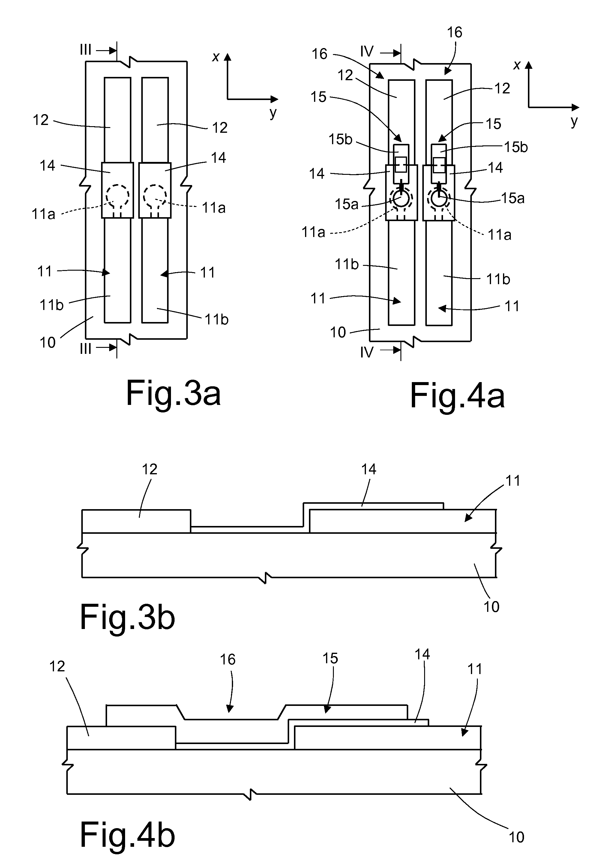
[0040]In detail (FIG. 13), during a single process of photolithography and etching of a layer of transparent conductive material, for example ITO, the first electrodes 11 and the electrical contacts 12 are initially formed on the substrate 10. The first electrodes 11 include active portions 11a, which are here to form row contacts of the array, and biasing portions 11b, each designed to bias a different row of the array. As will be clarified, each of the electrical contacts 12 enables biasing of a respective column of the array.

[0041]Then (FIG. 14), the organic regions 14 are formed (again via a selective patterning process) in the area corresponding to the intersections between the rows of the array, defined by the active portions 11a, and the columns of the array, defined ideally by the prolongations of the electrical contacts 12.

[0...


PUM


Abstract

An encapsulated organic electronic device is provided with: a substrate; at least one first elementary component and one second elementary component set above the substrate, each of said first and second elementary components being provided with a respective first electrode set above the substrate, a respective region of organic material set above the first electrode, and a respective second electrode set above the region of organic material at least partially in an area corresponding to the first electrode; and an encapsulation structure, defining an encapsulation space isolated from an external environment and designed to protect the first and second elementary components from the external environment. In particular, the regions of organic material of the first and second elementary components are separated and distinct from one another and are set entirely within the encapsulation space.

Description

PRIORITY CLAIM[0001]The present application claims the benefit of Italian Patent Application Serial No. TO2007U 000116, filed Sep. 11, 2007, which application is incorporated herein by reference in its entirety.TECHNICAL FIELD[0002]Embodiments of the present invention relate to an encapsulated organic electronic device and to a corresponding manufacturing process such as the manufacturing of organic LED devices (Organic Light-Emitting Diodes (OLEDs).BACKGROUND[0003]As is known, the use of organic semiconductor materials has proven very promising for the production of electronic and optoelectronic devices such as, for example, photovoltaic devices, OLEDs, thin-film transistors (TFTs), solid-state lasers, and sensors. For example, OLED devices are currently used as functional units for the production of displays formed by an array of luminous pixels that can be addressed separately.SUMMARY[0004]In a known manner, and as shown in FIG. 1, an OLED component 1 generally comprises: a subst...

Claims


Application Information

Patent Timeline
IPC IPC(8): H01J1/63H01L51/00H01L51/40
CPCH01L27/3281H01L51/5237H01L51/5203H10K59/17H10K50/805H10K50/841
Inventor TASSINI, PAOLOMAGLIONE, MARIA GRAZIAROMANELLI, EMMAVACCA, PAOLOMINARINI, CARLA
Owner STMICROELECTRONICS SRL
Why Eureka
Try Eureka