Nanowire multispectral imaging array

a multi-spectral imaging and array technology, applied in the field of infrared detectors and imaging arrays, can solve the problems of high vacuum, inability to meet the sensitivity of individual microbolometer pixels, and inability to respond uniformly to infrared radiation, so as to increase the manufacturability of multi-spectral imaging array systems and reduce thermal time constants , the effect of high frame ra

Active Publication Date: 2009-03-19
HONEYWELL INT INC
View PDF20 Cites 46 Cited by
  • Summary
  • Abstract
  • Description
  • Claims
  • Application Information

AI Technical Summary

Benefits of technology

[0015]A multispectral imaging array system, comprising a substrate and a plurality of antennas located with respect to one another on the substrate, such that a plurality of respective gaps are formed between each antenna among the plurality of antennas, wherein each group of antennas among the plurality of antennas comprises a different antenna size. Additionally, one or more nanowires can be located one or more gaps among the respective gaps, such that the nanowires in communication with the antennas and the substrate comprise a multispectral imaging system in which the use of the nanowire(s) decreases the thermal time constant and therefore the read out rate from the antennas while decreasing the ambient gas cooling speed relative to the read out rate to increase the manufacturability of the multispectral imaging array system.
[0016]The disclosed embodiments demonstrate how to obtain the high frame rate for high pixel count by using the nanowires as the microbolometer sensing element. The nanowire allows for using the antennas printed on the same dielectric substrate with the size covering the broad spectral range (e.g. 0.8-54 THz) because it replaces microbridge and can be scaled in length to match the gap between the antennas as it changes for different frequency ranges. Moreover the very small diameter of the nanowire decreases the thermal time constant and therefore increases the read-out rate. At the same time the nanowire small diameter decreases the ambient gas cooling speed relative to the read-out rate in the package which increases the required pressure in the package and therefore makes the vacuum package more manufacturable. The material properties of the nanowire can be selected to provide multiple wires in each sensor and therefore decrease the manufacturing variation of the sensor. The basic difference from the other microbolometer arrays is that the microbridge sensing element is replaced by the nanowire for both resistive and thermo-electric implementations.
[0017]In one embodiment, four different antenna sizes can be printed on the same substrate and the nanowires can be placed in the gap between the antennas. There are four antenna sizes because each antenna can be tuned only to a limited bandwidth. The gap size has to be of the order of 1 / 10 of the wavelength and therefore the nanowire length is smaller for higher frequencies. The manufacturing process consists of printing the antennas on the thin dielectric layer on a ground plane substrate. Then the nanowires are deposited in the gaps between the antennas. It is followed by making local packages over each antenna gap. The package protects the fragile nanowire and creates low enough ambient pressure so the gas cooling time constant is longer than the read-out time constant. The readout electronics may be either made of the nanowires or added to the array later on separate die. The electrical connection and vias between pixels and the electronics are printed.

Problems solved by technology

The quality of the vacuum inside the package greatly affects the sensitivity of the detector, a high vacuum being necessary.
Individual microbolometer pixels will have non-uniform responses to uniform incident infrared radiation, even when they are manufactured as part of a single microbolometer FPA.
Prior art systems and configurations have not effectively achieved this goal.

Method used


Image

  • Nanowire multispectral imaging array
  • Nanowire multispectral imaging array
  • Nanowire multispectral imaging array

Examples


Embodiment Construction

[0021]The particular values and configurations discussed in these non-limiting examples can be varied and are cited merely to illustrate at least one embodiment of the present invention and are not intended to limit the scope of the invention.

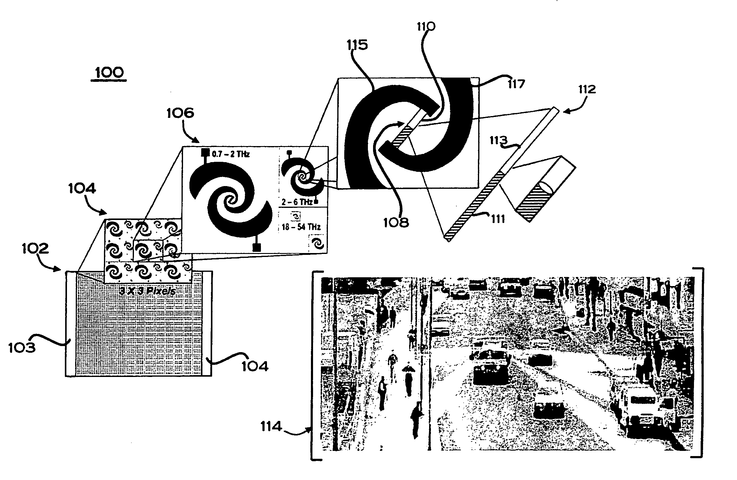
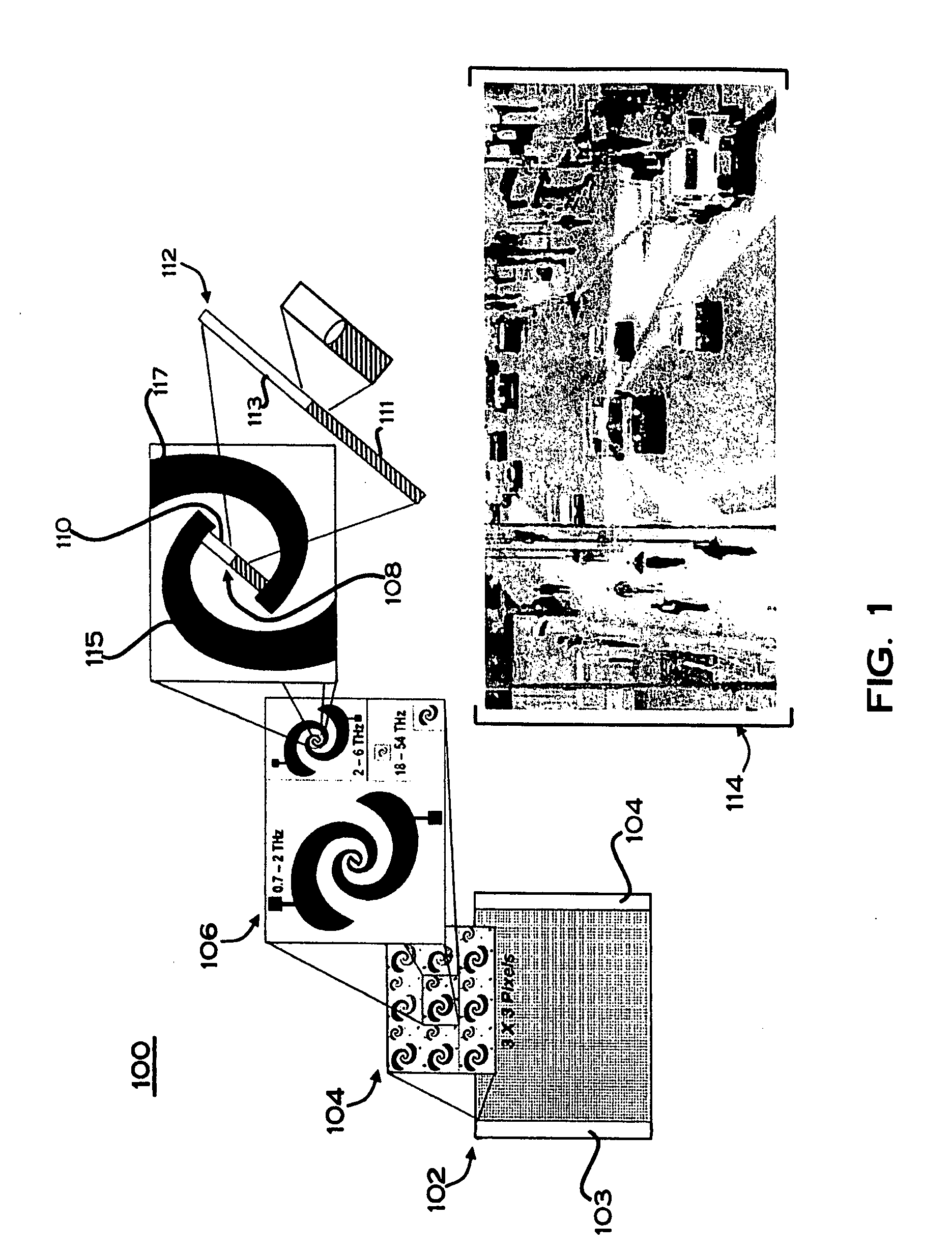
[0022]The embodiments disclosed herein describe how to obtain a high frame rate for a high pixel count by utilizing nanowires as the microbolometer sensing element. The nanowire(s) allows for using antennas printed on the same dielectric substrate with a size covering a range of 0.8-54 THz because it effectively replaces the microbridge and can be scaled in length to match the gap between the antennas. Moreover the very small diameter of the nanowire decreases the thermal time constant and therefore increases the read-out rate.

[0023]At the same time, the nanowire small diameter decreases the ambient gas cooling speed relative to the read-out rate in the package which makes the vacuum package more manufacturable. The material properties of the n...


PUM


Abstract

A multispectral imaging array system and method of forming the same. A substrate and a group of antennas can be located with respect to one another on the substrate, such that respective gaps are formed between each antenna group and wherein different antenna sizes may be used for different spectral ranges. Additionally, one or more nanowires can be located within one or more gaps among the respective gaps, such that the nanowires in communication with the antennas and the substrate comprise a multispectral imaging system in which the use of the nanowire(s) decreases the thermal time constant and therefore the read out rate from the antennas while decreasing the ambient gas cooling speed relative to the read out rate to increase the manufacturability of the multispectral imaging array system.

Description

CROSS-REFERENCE TO PROVISIONAL PATENT APPLICATION[0001]This application claims the benefit of U.S. Provisional Patent application Ser. No. 60 / 972,120, entitled “Nanowire Multispectral Imaging Array”, which was filed on Sep. 13, 2007.TECHNICAL FIELD[0002]Embodiments are generally related to imaging arrays and infrared detectors. Embodiments are also related to microbolometers and imaging systems that employ microbolometer components. Embodiments are also related to nanowires and nanotechnology-based components.BACKGROUND OF THE INVENTION[0003]Infrared (IR) detectors are often utilized to detect fires, overheating machinery, planes, vehicles, people, and any other objects that emit thermal radiation. Infrared detectors are unaffected by ambient light conditions or particulate matter in the air such as smoke or fog. Thus, infrared detectors have potential use in night vision and when poor vision conditions exist, such as when normal vision is obscured by smoke or fog. IR detectors are ...

Claims


Application Information

Patent Timeline
Patent Type & Authority Applications(United States)
IPC IPC(8): G01J5/02
CPCB82Y20/00G01J3/36G01J5/02G01J5/024G01J5/08H01L27/14669G01J5/0853G01J5/0884G01J5/24G01J2005/0077G01J5/0837
Inventor PECZALSKI, ANDY M.COLE, BARRETT E.
Owner HONEYWELL INT INC
Why Eureka
Try Eureka