Semiconductor detection module and radiation detection apparatus and radiological imaging apparatus using the semiconductor detection module

a detection module and semiconductor technology, applied in the direction of x/gamma/cosmic radiation measurement, radiological control devices, instruments, etc., can solve the problems of deteriorating workability, difficult to achieve simultaneous high energy resolution and high density detection apparatus, etc., to achieve excellent energy resolution and high energy resolution. , the effect of high sensitiv

Inactive Publication Date: 2009-03-19
HITACHI LTD
View PDF4 Cites 4 Cited by
  • Summary
  • Abstract
  • Description
  • Claims
  • Application Information

AI Technical Summary

Benefits of technology

[0018]The present invention is capable of achieving semiconductor detection modules each having a structure in which detection devices, which are densely disposed, are highly sensitive, and have excellent energy resolution, can be

Problems solved by technology

This problem makes it impossible to simultaneously achieve both a high energy resolution and a high density detection apparatus (position resolution).
Thi

Method used


Image

  • Semiconductor detection module and radiation detection apparatus and radiological imaging apparatus using the semiconductor detection module
  • Semiconductor detection module and radiation detection apparatus and radiological imaging apparatus using the semiconductor detection module
  • Semiconductor detection module and radiation detection apparatus and radiological imaging apparatus using the semiconductor detection module

Examples


first embodiment

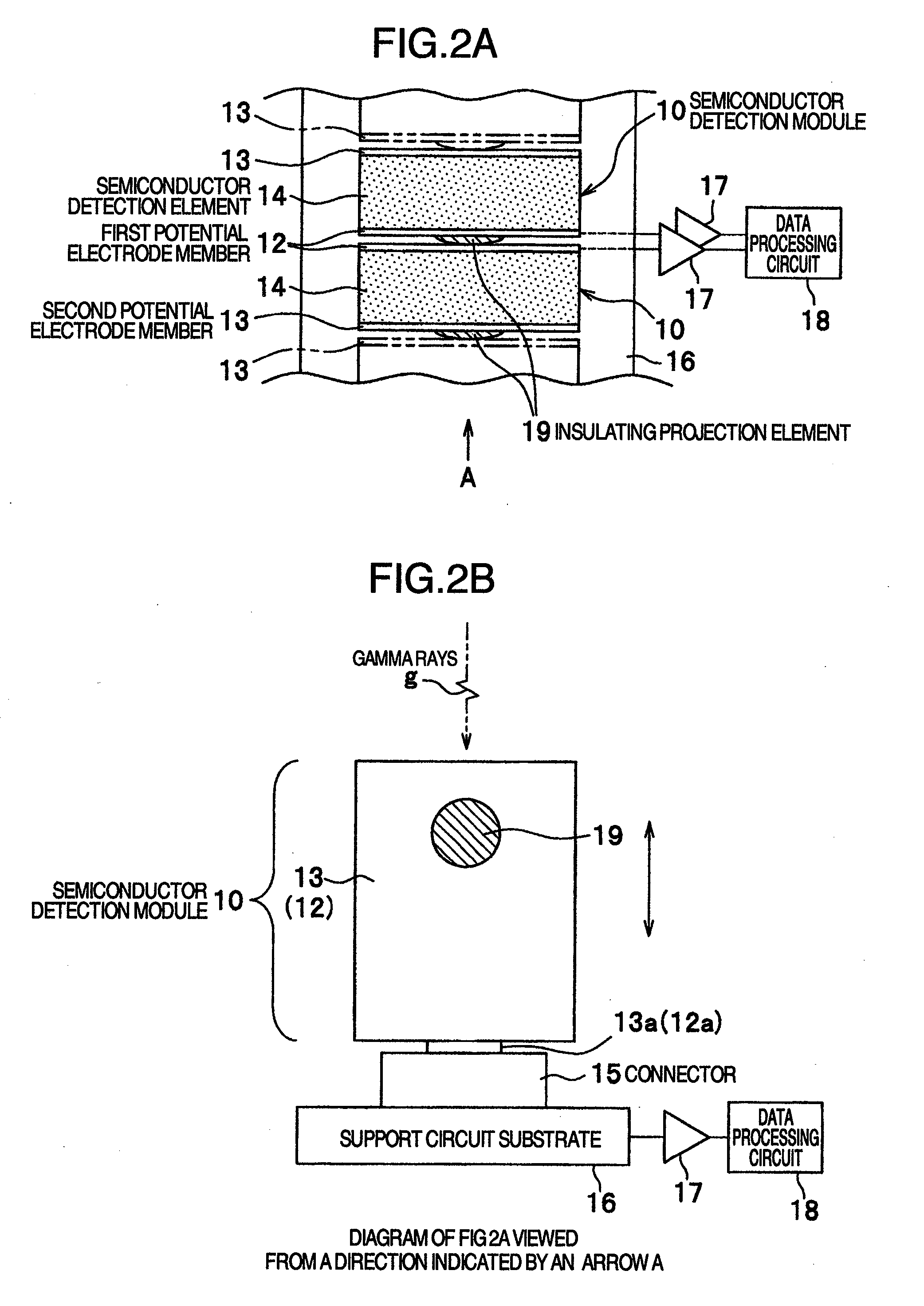
[0044]FIGS. 2A and 2B show single pixel-type semiconductor detection modules 10 according to a first embodiment. FIG. 2A is a top view of the semiconductor detection modules 10 viewed from a direction in which the gamma rays g shown in FIG. 1 enter the semiconductor detection elements 14 of the semiconductor detection modules 10. FIG. 2B is a diagram of the semiconductor modules 10 of FIG. 2A viewed from a direction indicated by an arrow A.

[0045]Each of the semiconductor detection modules 10 shown in FIGS. 2A and 2B has one or more semiconductor detection elements 14. Each of the semiconductor detection elements 14, as one pixel, reads a signal generated by the entrance of the gamma rays g. In addition, each of the semiconductor detection elements 14 is provided with a first potential electrode member 12 and a second potential electrode member 13 on both ends thereof. An insulating projection element 19 comprised of an insulator, which will be described later, is disposed between th...

second embodiment

[0062]FIGS. 3A to 3C show matrix reading type semiconductor detection modules 20 according to a second embodiment of the present invention.

[0063]FIG. 3A is a top view of the semiconductor detection modules 20 viewed from the direction in which the gamma rays g shown in FIG. 1 enter semiconductor detection elements 24 of the semiconductor detection modules 20. FIG. 3B is a diagram of the semiconductor detection modules 20 viewed from an direction indicated by an arrow B. FIG. 3C is a diagram of the semiconductor detection modules 20 viewed from an direction indicated by an arrow C. FIG. 4 is a top view of a support circuit substrate 26 in which connectors (fixation means) 25a, 25b for installing the semiconductor detection modules 20 shown in FIGS. 3A to 3C are standingly provided.

[0064]FIG. 3A shows the disposed matrix read-type semiconductor detection modules 20 by two solid lines.

[0065]As FIG. 3A shows, the matrix read-type semiconductor detection modules 20 each comprises: a plur...


PUM


Abstract

Semiconductor detection modules 10 according to the present invention each comprises: one or more semiconductor detection elements 14 that receive radiation to generate induced charges as signals; and a pair of electrodes 12, 13 that are disposed to sandwich the one or more semiconductor elements 14, and obtains a data signal that is generated by the entrance of radiation into the semiconductor elements 14. In each of the semiconductor detection modules 10, a partial insulator 19 having an area smaller than that of the pair of electrodes 12, 13 is provided on at least one of the pair of electrodes 12, 13 at a place between the one electrode 12 and adjacent another electrodes 12, and between the one electrode 13 and adjacent another electrodes 13.

Description

BACKGROUND OF THE INVENTION[0001]The present invention relates to semiconductor detection modules in which semiconductor radiation detection elements can be replaced, and to a radiation detection apparatus or a radiological imaging apparatus or a nuclear medicine diagnostic apparatus, such as a single photon emission computer tomography apparatus (referred as a SPECT apparatus hereinafter) or a positron emission tomography apparatus (referred to as a PET apparatus hereinafter), using the semiconductor detection modules.[0002]As a radiation detection apparatus for detecting radiation such as gamma rays, one using a NaI scintillator has conventionally been known.[0003]FIG. 5 is a conceptual cross-sectional diagram showing an internal construction of a gamma camera 100 having a NaI scintillator 101.[0004]As FIG. 5 shows, in the gamma camera 100 having the NaI scintillator 101, which is a kind of a nuclear medicine diagnostic apparatus, gamma rays 109 which are a form of radiation enter...

Claims


Application Information

Patent Timeline
IPC IPC(8): G01T1/24
CPCG01T1/243G01T1/249
Inventor YOKOI, KAZUMAISHITSU, TAKAFUMIAMEMIYA, KENSUKE
Owner HITACHI LTD
Why Eureka
Try Eureka