Interconnect Structures Incorporating Air-Gap Spacers

a technology of interconnect structure and air gap, which is applied in the direction of solid-state devices, basic electric elements, instruments, etc., can solve the problems of poor interconnect breakdown behavior, affecting chip speed and thus chip performance, and generally difficult to achieve, so as to facilitate a quick pinch

Inactive Publication Date: 2009-03-19
TESSERA INC
View PDF14 Cites 71 Cited by
  • Summary
  • Abstract
  • Description
  • Claims
  • Application Information

AI Technical Summary

Benefits of technology

[0024]For damaged ILD widths of approximately >30 nm, for which the likelihood of subsequent cap deposition filling the air-gap created after the selective etch is high, we propose a second embodiment of the present invention. The relevant air-width could range from about 30 nm and larger. However, the exact limits depend on the cap deposition method and would be obvious to those skilled in the art. In the second embodiment, the cap layer is deposited following CMP. Perforations are made in the cap layer either by using an optical mask or by using a random self-assembled scheme as outli

Problems solved by technology

Because of their effects on signal propagation delays, the materials and layout of these interconnect structures can substantially impact chip speed, and thus chip performance.
This is generally very difficult to achieve.
This is an undesirable structure since it could lead to high field concentrations around the curved parts and poor breakdown behavior of the interconnect, a significant drawback.
This makes their scheme very expensive and limits the performance due to their inability to extend the air-gap below the trench to obtained increased performance.
Finally, in their scheme, they use plasma based methods to remove the dielectric spacer to form the air-gap and they do this with the metal interconnect already present in the structure which could lead to a degradation of the conductive properties of the interconnect.
The other drawbacks mentioned above for U.S. Pat. No. 6,228,763 still remain, the chief of which is that this is based on a single damascene integration scheme which is prohibitively expensive, limited in performance, and not extendible readil

Method used


Image

  • Interconnect Structures Incorporating Air-Gap Spacers
  • Interconnect Structures Incorporating Air-Gap Spacers
  • Interconnect Structures Incorporating Air-Gap Spacers

Examples


Embodiment Construction

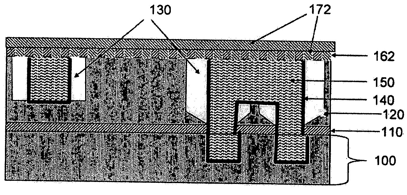
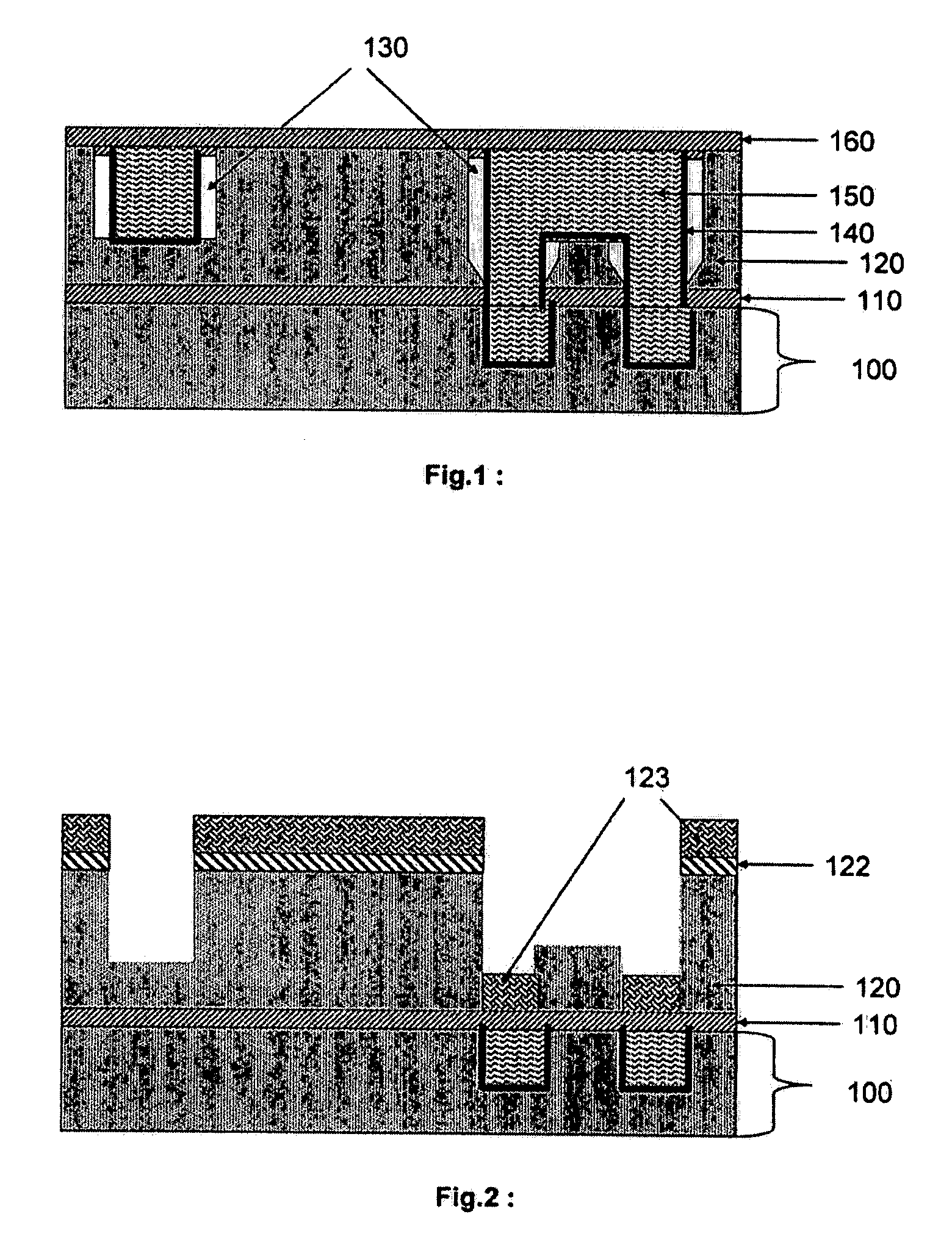
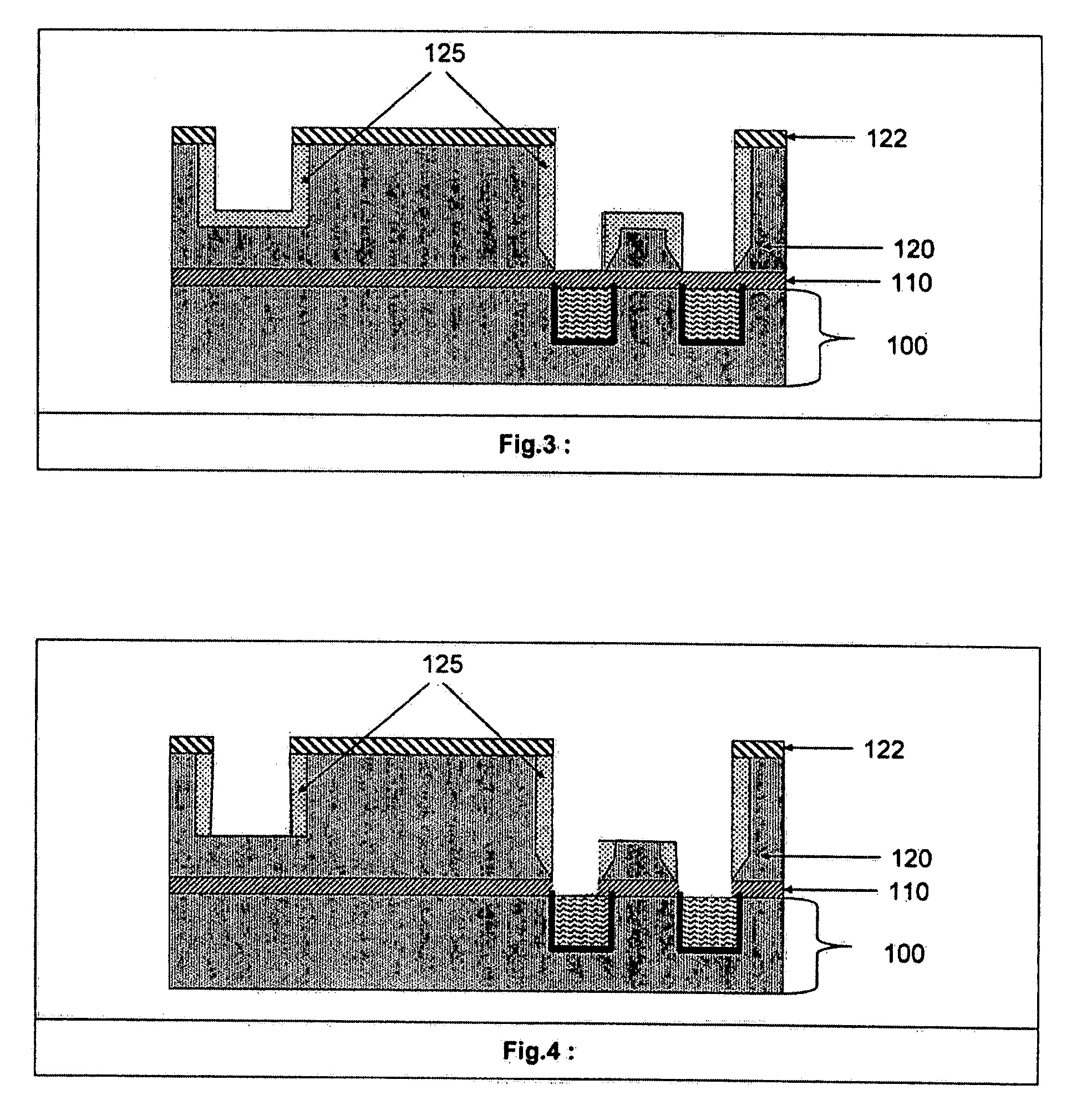
[0038]The process sequence used to generate the interconnect structures with air-gap spacers is described with reference to the accompanying drawings. FIG. 1 shows a schematic cross section view of the proposed air-gap interconnect structure, the left side of FIG. 1 illustrating the placement of a trench and the right side, the placement of a combined or stacked trench and via contiguous to one another and having a common axis, with the trench configuration comprising the top of the structure and the via at the bottom. A two level structure is shown with 100 representing an underlying build with a dielectric material 120. A cap layer, 110, is deposited on this level and a dual damascene interconnect build with air-gap spacers is shown. The structure is comprised of the following: 120 is the dielectric material and is a porous or dense material comprised of silica or an organosilicate. The air-gaps are represented by 130 and depending on the metal structure may be limited to the line...


PUM


Abstract

A dual damascene article of manufacture comprises a trench containing a conductive metal column where the trench and the conductive metal column extend down into and are contiguous with a via. The trench and the conductive metal column and the via have a common axis. These articles comprise interconnect structures incorporating air-gap spacers containing metal/insulator structures for Very Large Scale Integrated (VLSI) and Ultra Large Scale Integrated (ULSI) devices and packaging. The trench in this regard comprises a sidewall air-gap immediately adjacent the side walls of the trench and the conductive metal column, the sidewall air-gap extending down to the via to a depth below a line fixed by the bottom of the trench, and continues downward in the via for a distance of from about 1 Angstrom below the line to the full depth of the via. In another aspect, the article of manufacture comprises a capped dual damascene structure.

Description

FIELD OF THE INVENTION[0001]The field of the invention comprises semiconductor device manufacturing and more specifically to methods of forming air-gap containing metal / insulator interconnect structures for Very Large Scale Integrated (VLSI) and Ultra Large Scale Integrated (ULSI) devices and packaging.BACKGROUND OF THE INVENTION[0002]Device interconnections in Very Large Scale Integrated (VLSI) or Ultra-Large Scale Integrated (ULSI) semiconductor chips typically have multilevel structures containing patterns of metal wiring layers encapsulated in an insulator. Wiring structures within a given level of wiring are separated by an intra level dielectric, while the individual wiring levels are separated from each other by layers of an inter level dielectric conductive vias are formed in the inter level dielectric to provide inter level contacts between the wiring traces.[0003]Because of their effects on signal propagation delays, the materials and layout of these interconnect structure...

Claims


Application Information

Patent Timeline
IPC IPC(8): H01L23/52
CPCH01L21/76808H01L21/7682H01L21/76832H01L21/76834H01L23/5222H01L23/53238H01L2924/0002H01L23/5329H01L23/53295H01L2924/00H01L2221/1063G01H3/00G01H11/00G01H11/02G01H11/06H01L23/481H01L23/52H01L23/5226H01L23/522H01L23/48H01L21/76843H01L21/31111H01L21/76802H01L21/76826H01L21/76831H01L21/76877H01L21/76807H01L21/76829
Inventor NITTA, SATYA V.PONOTH, SHOM
Owner TESSERA INC
Why Eureka
Try Eureka