Unlock instant, AI-driven research and patent intelligence for your innovation.

Bonding agent sticking inspection apparatus, mounting apparatus, and method of manufacturing electrical component

Active Publication Date: 2009-03-19
KK TOSHIBA
View PDF3 Cites 7 Cited by
  • Summary
  • Abstract
  • Description
  • Claims
  • Application Information

AI Technical Summary

Benefits of technology

[0021]An object of the present invention is to provide a bonding agent sticking inspection apparatus capable of accurately judging a nick of a bonding agent which hinders the electrical connection. Another object of the present invention is to provide a mounting apparatus including a bonding agent sticking inspection apparatus capable of accurately judging a nick of a bonding agent which hinders the electrical connection. Still another object of the present invention is to provide a method of manufacturing an electrical component capable of accurately judging a nick of a bonding agent which hinders the electrical connection.

Problems solved by technology

Particularly, when the base tape is removed after the bonding agent is stuck on the liquid crystal pane, the peripheral edge part of the bonding agent is liable to be chipped off.
When no bonding agent is interposed between the electrode and the semiconductor chip, or between the electrode and the flexible substrate, the electrical connection at these parts is liable to be canceled.
The bonding agent is cut when it is stuck, and the base tape is peeled off from the cut end part of the bonding agent, and hence a nick is liable to occur at the end part.
However, it can be considered that a nick may occur at parts other than the both end parts, and hence inspecting the entire bonding agent is performed.
Conversely, when the size of the nick is larger than the threshold, and the nick has a shape overlapping, for example, an electrode, it becomes impossible for the electrode to be connected to the semiconductor chip or the flexible substrate.
Thus, as described above, it is considered that even when a shape of the nick is a shape that does not hinder the electrical connection, it may possibly be judged that there is an abnormality in the bonding agent.
It is therefore not desirable that the bonding agent be judged as abnormal if the nick does not hinder the electrical connection.

Method used


Image

  • Bonding agent sticking inspection apparatus, mounting apparatus, and method of manufacturing electrical component
  • Bonding agent sticking inspection apparatus, mounting apparatus, and method of manufacturing electrical component
  • Bonding agent sticking inspection apparatus, mounting apparatus, and method of manufacturing electrical component

Examples


Embodiment Construction

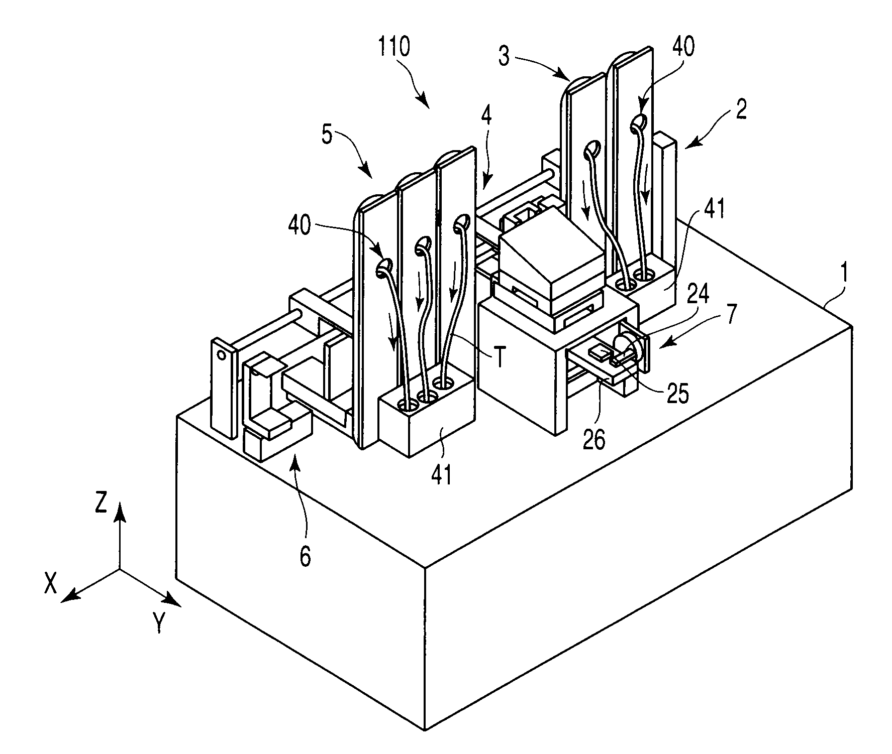
[0056]A mounting apparatus 110 according to an embodiment of the present invention will be described below with reference to FIGS. 1 to 19. FIG. 1 is a schematic view showing a mounting system 100 for mounting a semiconductor chip H or a flexible substrate 61 on a liquid crystal panel 121.

[0057]As shown in FIG. 1, the mounting system 100 is provided with a liquid crystal panel supply unit 120 for supplying a liquid crystal panel 121, a washing unit 130 for washing the liquid crystal panel 121, an IC mounting unit 140 for mounting a semiconductor chip H on the liquid crystal panel 121, a buffer unit 150, an FPC mounting unit 160 for mounting a flexible substrate 61 on the liquid crystal panel 121, an IC supply unit 142 for supplying a semiconductor chip H to the IC mounting unit 140, an FPC supply unit 162 for supplying a flexible substrate 61 to the FPC mounting unit 160, a liquid crystal panel collection unit 170 for collecting the liquid crystal panel 121 which has been subjected ...


PUM


Abstract

A bonding agent sticking inspection apparatus includes a photographing section, a movement section, and a control section. The photographing section photographs an image of a substrate. The image includes a sticking expected range indicating a range in which a bonding agent should be positioned. The control section controls the photographing section and the movement section, sets an inspection region having a width equal to the pitch between electrodes in an entire edge part in a direction in which the electrodes are arranged in a peripheral edge part of the sticking expected range in the image, detects a ratio of a nicked part of the bonding agent to the inspection region, and judges whether or not an abnormality is present in the bonding agent on the basis of a comparison between the ratio of the nicked part and a threshold set in advance.

Description

CROSS-REFERENCE TO RELATED APPLICATIONS[0001]This application is based upon and claims the benefit of priority from prior Japanese Patent Application No. 2007-238446, filed Sep. 13, 2007, the entire contents of which are incorporated herein by reference.BACKGROUND OF THE INVENTION[0002]1. Field of the Invention[0003]The present invention relates to a bonding agent sticking inspection apparatus for inspecting a sticking state of a bonding agent such as an anisotropic conductive film stuck on a glass substrate of, for example, a liquid crystal panel. Further, the present invention relates to a mounting apparatus provided with a bonding agent sticking inspection apparatus for inspecting a sticking state of a bonding agent such as an anisotropic conductive film stuck on a glass substrate of, for example, a liquid crystal panel. Furthermore, the present invention relates to a method of manufacturing an electrical component including a bonding agent sticking inspection step for inspecting...

Claims


Application Information

Patent Timeline
IPC IPC(8): G01B11/00H01L21/66
CPCH05K1/0269H05K2203/163H05K2201/09918H05K3/323
Inventor KOBAYASHI, DAISUKE
Owner KK TOSHIBA
Features
  • R&D
  • Intellectual Property
  • Life Sciences
  • Materials
  • Tech Scout
  • Unparalleled Data Quality
  • Higher Quality Content
  • 60% Fewer Hallucinations
Learn More