Semiconductor storage device and operating method of the same

a technology of semiconductor storage and operating method, which is applied in semiconductor devices, digital storage, instruments, etc., can solve the problems of output shifting, difficulty in accurately evaluating the resistance value of one storage element, and difficulty in employing it for making a higher-capacity memory with a hyperfine structure. , to achieve the effect of high integration, high speed reading, and high capacity

Active Publication Date: 2009-03-19
NEC CORP
View PDF13 Cites 8 Cited by
  • Summary
  • Abstract
  • Description
  • Claims
  • Application Information

AI Technical Summary

Benefits of technology

[0020]Also, another object of the present invention is to provide a semiconductor storage device in which high speed reading, miniaturization and a high capacity can be attained while a high integration is attained by using a switch element shared by a plurality of storing elements, and an operating method of the same.

Problems solved by technology

However, since the area of the selection transistor and the area for the connection are required, it is difficult to employ it for making a higher-capacity memory with a hyperfine structure.
However, since all of the storage elements are connected in parallel, it is difficult to accurately evaluate the resistance value of one storage element.
However, actually, the EP method has a problem that the output is shifted, depending on the wiring resistance.
However, since the wiring length becomes long, the read current difference is further reduced, which makes the reading difficult.

Method used


Image

  • Semiconductor storage device and operating method of the same
  • Semiconductor storage device and operating method of the same
  • Semiconductor storage device and operating method of the same

Examples


first exemplary embodiment

[0062]The first exemplary embodiment of the semiconductor storage device of the present invention will be described below with reference to the attached drawings.

[0063]FIG. 4 is a block diagram showing a configuration of the first exemplary embodiment of the semiconductor storage device of the present invention. A semiconductor storage device 20 includes a resistive storage element array 21, a plurality of evaluating circuits 8-1 to 8-m (hereafter, m is a natural number), an evaluation control circuit 9 and a reading control circuit 10.

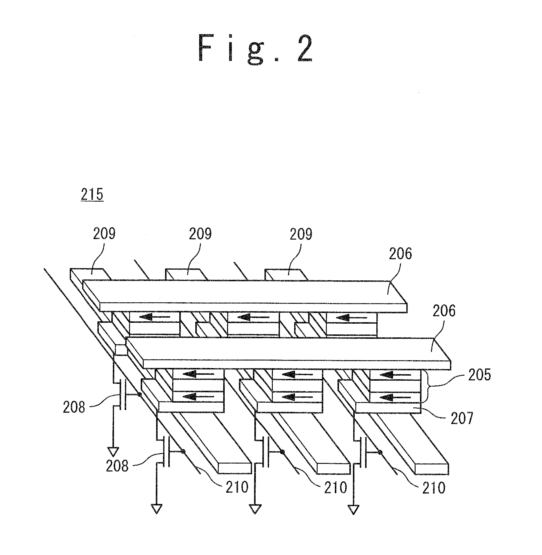
[0064]The resistive storage element array 21 includes a plurality of unit blocks 4-1 to 4-p (hereafter, p is a natural number). Each of the plurality of unit blocks 4-1 to 4-p includes a plurality of memory cells M11 to Mnm (hereafter, n is a natural number), a plurality of word lines 2-1 to 2-n, a plurality of bit lines 5-1 to 5-m, a plurality of assistant bit lines 3-1 to 3-m, a plurality of switch elements 6-1 to 6-m, and a switch element control l...

first example

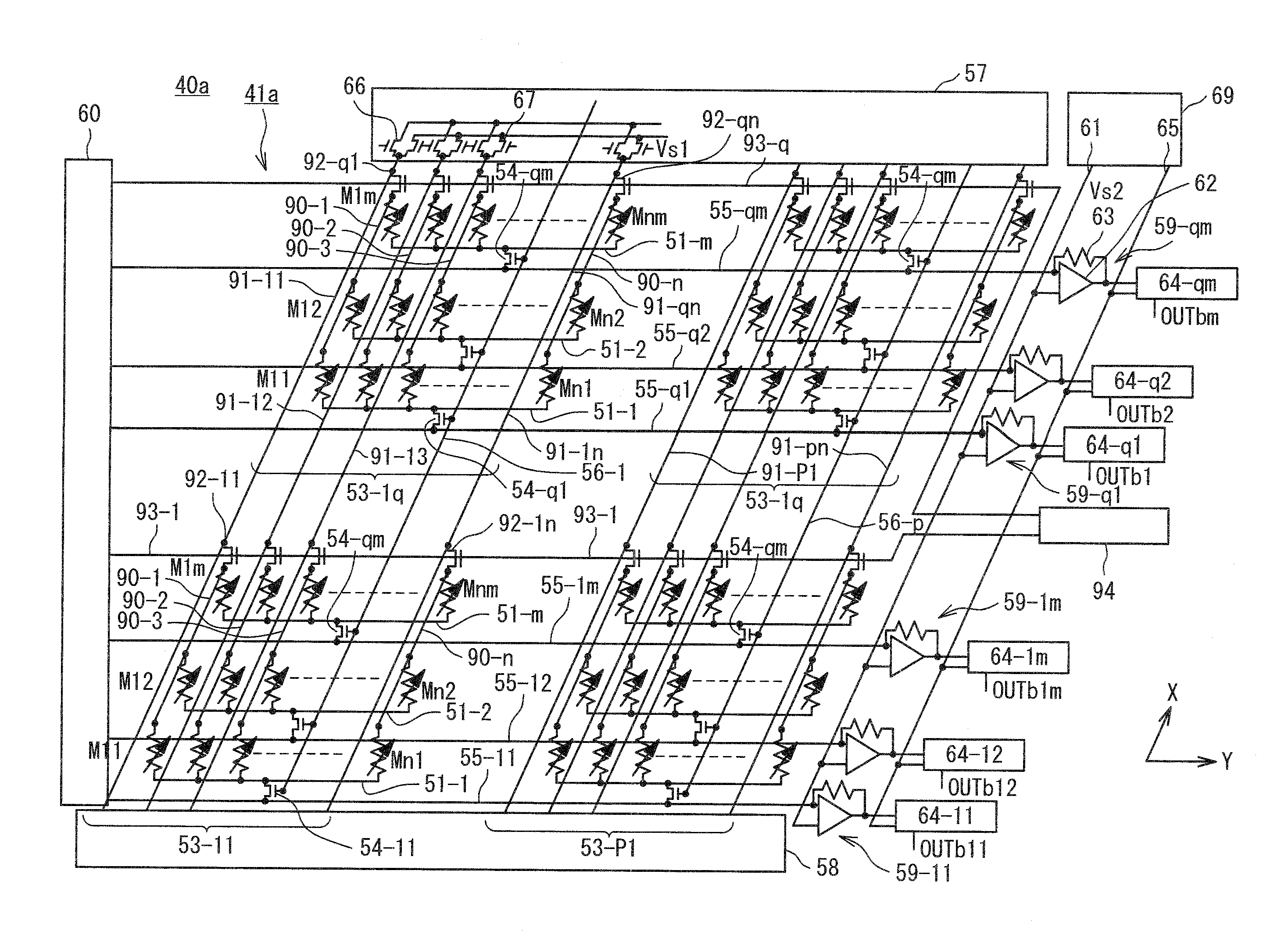
[0084]The exemplary embodiment of the present invention will be described below using an specific example. FIG. 7 is a schematic configuration view showing a first example of the semiconductor device of the present invention. FIG. 8 is a main sectional view of a TMR element 52 in FIG. 7. A semiconductor storage device 40 includes a resistive storage element array 41, a plurality of sensing amplifiers 64-1 to 64-m, an evaluation control circuit 69, a word line control circuit 57, a word line termination circuit 58, a bit line termination circuit 60, and a plurality of potential setting circuits 59.

[0085]The resistive storage element array 41, unit blocks 53-1 to 53-p, memory cells M11 to Mnm, the TMR element 52, a plurality of word lines 50-1 to 50-n, a plurality of bit lines 55-1 to 55-m, a plurality of assistant bit lines 51-1 to 51-m, a plurality of reading transistors 54-1 to 54-m, a block selection line 56, and sensing circuits 64-1 to 64-m correspond to the resistive storage el...

second example

[0099]FIG. 7 is the schematic configuration view showing a second example of the semiconductor device of the present invention. FIG. 11 is a main sectional view of the TMR element 52 in FIG. 7. The semiconductor device in the second example is substantially equal in the circuit configuration to the first example. However, the configuration of the storing element 52 and the operation of the word line control circuit 57 and the writing method are different.

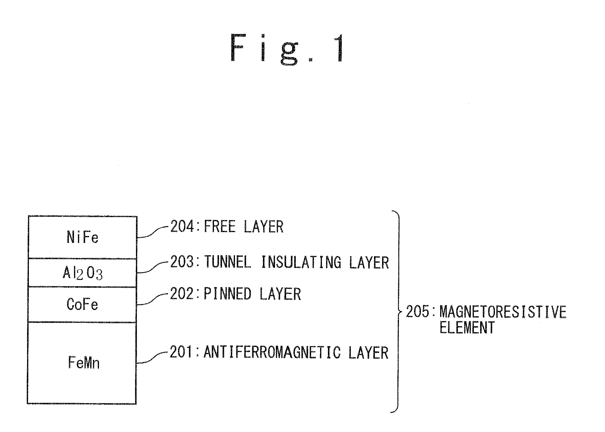
[0100]In the storing element 52, a lower wiring layer 81 (Ta: 10 nm), an anti-ferromagnetic layer 82 (PtMn / NiFe: 10 nm), a pinned layer 83 (CoFe: 2.4 nm), a first tunnel insulating layer 84 (Al2O3: 2 nm), a free layer 85 (CoFe: 2.4 nm), a second tunnel insulating layer 86 (Al2O3: 2 nm), a write magnetic layer 87 (NiFe: 5 nm), and an upper wiring layer 88 (Ta: 10 nm) are laminated in this order from the lower layer.

[0101]The operating method of the semiconductor storage device 40 will be described below exemplifying the case of using...


PUM


Abstract

A semiconductor storage device includes: reading blocks; third wirings; reading switches; a control circuit; and evaluating circuits. The reading blocks includes first and second wirings extended in a first and second direction, respectively, and resistive storage elements arranged at points where the first and second wirings intersect. The third wirings is extended in the second direction and provided correspondingly to the second wirings. The reading switches are arranged between the third and second wirings. The control circuit controls the reading switches and supplies currents or the like to the first wirings. The evaluating circuits are connected to the third wirings and evaluate the currents or the like. When data is read out, the control circuit selects a selection reading block and a selection first wiring and supplies the currents or the like, and the evaluating circuits execute the evaluations of the currents or the like in the third wirings.

Description

TECHNICAL FIELD[0001]The present invention relates to a semiconductor storage device and an operating method of the same, and more particularly relates to a semiconductor storage device in which a resistive storage element is used as a memory cell, and an operating method of the same.BACKGROUND ART[0002]A semiconductor storage device (memory) is known in which a resistive storage element whose resistance value is changed based on its state is used as a memory cell. The magnetoresistive element and the phase-change resistive element are known as the resistive storage elements. The magnetoresistive element indicates a magnetoresistance effect such as an AMR (Anisotropic MagnetoResistance) effect, a GMR (Giant MagnetoReistance) effect and a TMR (Tunnel MagnetoResistance) effect. The phase-change resistive element uses a difference between crystalline properties caused by cooling speeds.[0003]At first, as one example of the magnetoresistive element, the TMR element will be described. Th...

Claims


Application Information

Patent Timeline
Patent Type & Authority Applications(United States)
IPC IPC(8): G11C11/00G11C8/00
CPCB82Y10/00H01L27/226G11C11/16G11C11/161G11C11/1673H10B61/20
Inventor KATOU, YUUKOU
Owner NEC CORP
Why Eureka
Try Eureka