Semiconductor device and method of manufacturing semiconductor device

a semiconductor device and semiconductor technology, applied in the direction of semiconductor devices, basic electric elements, electrical appliances, etc., can solve the problems of difficult preparation of low-voltage semiconductor devices drivable at low voltage, dielectric breakdown of gate insulating films, etc., to achieve the effect of further reducing gate capacitance, further reducing gate charge quantity, and not increasing the on-resistance of semiconductor devices

Active Publication Date: 2009-03-26
ROHM CO LTD
View PDF4 Cites 38 Cited by
  • Summary
  • Abstract
  • Description
  • Claims
  • Application Information

AI Technical Summary

Benefits of technology

[0044]When the thickness of the portion of the gate insulating film adjacent to the source region is larger than the thickness of the portion opposed to the body region on the side surface of the trench, the parasitic capacitance formed between the gate electrode and the source region can be reduced without increasing the on-resistance of the semiconductor device. Therefore, the gate capacitance can be further reduced, and the gate charge quantity can also be further reduced. Consequently, the semiconductor device can achieve the switching operation at a higher speed.

Problems solved by technology

If the thickness of the gate insulating film 106 is reduced, however, a voltage exceeding the withstand voltage of the gate insulating film 106 may be applied between the gate and the drain upon voltage application to the drain electrode 114, to result in dielectric breakdown of the gate insulating film 106.
Therefore, it has been difficult to prepare a low-voltage semiconductor device drivable at a low voltage.

Method used


Image

  • Semiconductor device and method of manufacturing semiconductor device
  • Semiconductor device and method of manufacturing semiconductor device
  • Semiconductor device and method of manufacturing semiconductor device

Examples


first embodiment

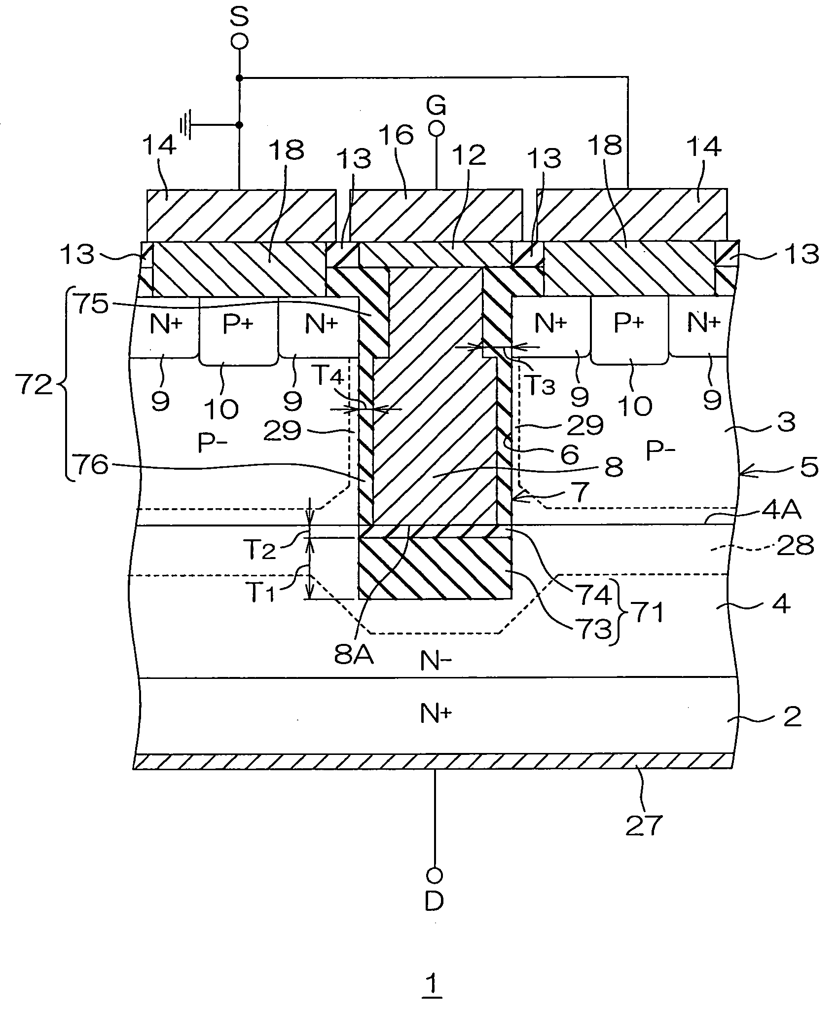
[0055]FIG. 1 is a schematic sectional view of a semiconductor device 1 according to the present invention.

[0056]The semiconductor device 1 has an array structure formed by arranging unit cells having trench gate VDMOSFETS in the form of a matrix.

[0057]On an N+-type substrate 2 forming the base of the semiconductor device 1, an N−-type layer 4 made of Si (silicon) doped with an N-type impurity (P (phosphorus), for example) in a lower concentration (1015 cm−3, for example) than the N+-type substrate 2 is laminated. A P−-type body region 5 is laminated on the N−-type layer 4.

[0058]A gate trench 6 is dug in the semiconductor device 1 from the surface of the body layer 5. The gate trench 6 passes through the body layer 5, so that the deepest portion thereof reaches the N−-type layer 4. A plurality of such gate trenches 6 are formed at regular intervals along the horizontal direction in FIG. 1, to extend in a direction (along the gate widths) perpendicular to the plane of FIG. 1 respectiv...

second embodiment

[0093]FIG. 3 is a schematic sectional view of a semiconductor device 31 according to the present invention. Referring to FIG. 3, portions corresponding to those shown in FIG. 1 are denoted by the same reference numerals. Further, redundant description is omitted as to the portions having the same reference numerals as the above.

[0094]In this semiconductor device 31, an N−-type layer 22 made of Si (silicon) doped with an N-type impurity in a lower concentration (1015 cm−3, for example) than an N+-type substrate 2 is laminated on the N+-type substrate 2. A P−-type body layer 5 is laminated on the N−-type layer 22.

[0095]A gate trench 6 is dug in the semiconductor device 31 from the surface of the body layer 5. The gate trench 6 passes through the body layer 5, so that the deepest portion thereof reaches the N−-type layer 22. A gate insulating film 35 made of SiO2 is formed on the inner surface of the gate trench 6 and the upper surface of the body layer 5, to cover the overall regions ...

third embodiment

[0117]FIG. 5 is a schematic sectional view of a semiconductor device 51 according to the present invention.

[0118]The semiconductor device 51 has an array structure formed by arranging unit cells having trench gate VDMOSFETS in the form of a matrix.

[0119]On an N+-type substrate 52 forming the base of the semiconductor device 51, an N−-type epitaxial layer 53 made of Si (silicon) doped with an N-type impurity in a lower concentration (1×1015 cm−3 to 4×1015 cm−3, for example) than the N+-type substrate 52 is laminated. The base layer portion of the epitaxial layer 53 forms an N−-type region 54 as a first conductivity type region in the state after the epitaxial growth. In the epitaxial layer 53, a P−-type body region 55 is formed on the N−-type region 54, in contact with the N−-type region 54.

[0120]A gate trench 56 is dug in the epitaxial layer 53 from the surface thereof. The gate trench 56 passes through the body region 55, so that the deepest portion thereof reaches the N−-type regi...


PUM


Abstract

A semiconductor device includes a first conductivity type layer of a first conductivity type, a body layer of a second conductivity type formed on the first conductivity type layer, a gate trench passing through the body layer so that the deepest portion thereof reaches the first conductivity type layer, a source region of the first conductivity type formed around the gate trench on the surface layer portion of the body layer, a gate insulating film formed on the bottom surface and the side surface of the gate trench, and a gate electrode embedded in the gate trench through the gate insulating film, and the bottom surface of the gate electrode and the upper surface of the first conductivity type layer are flush with each other.

Description

BACKGROUND OF THE INVENTION[0001]1. Field of the Invention[0002]The present invention relates to a semiconductor device having a trench gate VDMOSFET and a method of manufacturing a semiconductor device.[0003]2. Description of Related Art[0004]A trench gate structure is generally known as a structure effective for refinement of a VDMOSFET (Vertical Double diffused Metal Oxide Semiconductor Field-Effect Transistor).[0005]FIG. 9 is a schematic sectional view of a conventional semiconductor device 100 having a trench gate VDMOSFET.[0006]The semiconductor device 100 includes an N+-type substrate 101. An N−-type epitaxial layer 102 is laminated on the N+-type substrate 101. The base layer portion of the N−-type epitaxial layer 102 forms an N−-type region 103, while a P−-type body region 104 is formed on the surface layer portion of the N−-type epitaxial layer 102 vertically adjacently to the N−-type region 103.[0007]A gate trench 105 is dug in the N−-type epitaxial layer 102 from the sur...

Claims


Application Information

Patent Timeline
Patent Type & Authority Applications(United States)
IPC IPC(8): H01L21/336H01L29/78
CPCH01L29/0623H01L29/0878H01L29/41775H01L29/4236H01L29/7813H01L29/4925H01L29/512H01L29/66734H01L29/42368
Inventor NAKAGAWA, YOSHIKAZUIZUMI, NAOKINAGATA, MASAKI
Owner ROHM CO LTD
Why Eureka
Try Eureka