Wafer bonding activated by ion implantation

Active Publication Date: 2009-03-26
VARIAN SEMICON EQUIP ASSOC INC
View PDF6 Cites 220 Cited by
  • Summary
  • Abstract
  • Description
  • Claims
  • Application Information

AI Technical Summary

Benefits of technology

[0010]Exemplary embodiments of the present invention are directed to a wafer bonding method activated by ion implantation. In an exemplary embodiment, the method includes placing at least two substrates into an ion target chamber. At least one surface of a first of the two substrates is exposed to an ion beam. This exposure re

Problems solved by technology

In addition, plasma activation reduces the possibility for contamination as well as obviating the need for temperature annealing.
Use of a

Method used


Image

  • Wafer bonding activated by ion implantation
  • Wafer bonding activated by ion implantation
  • Wafer bonding activated by ion implantation

Examples


Embodiment Construction

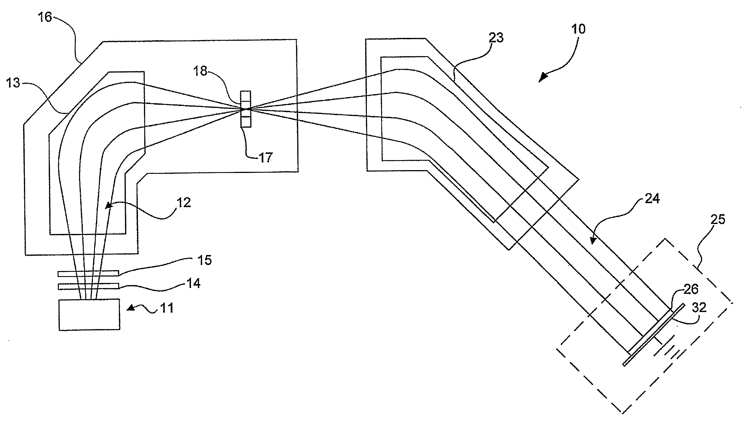
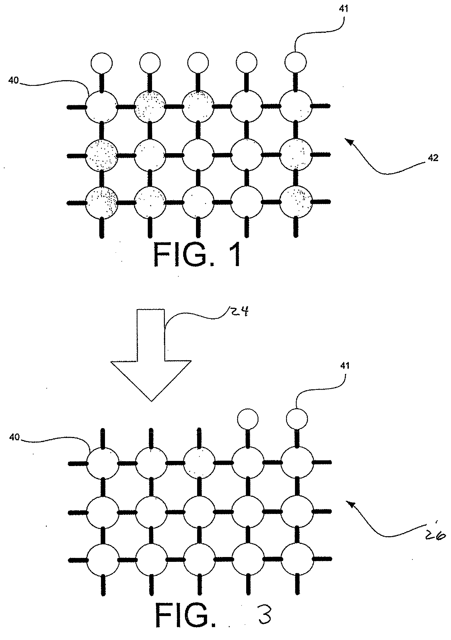
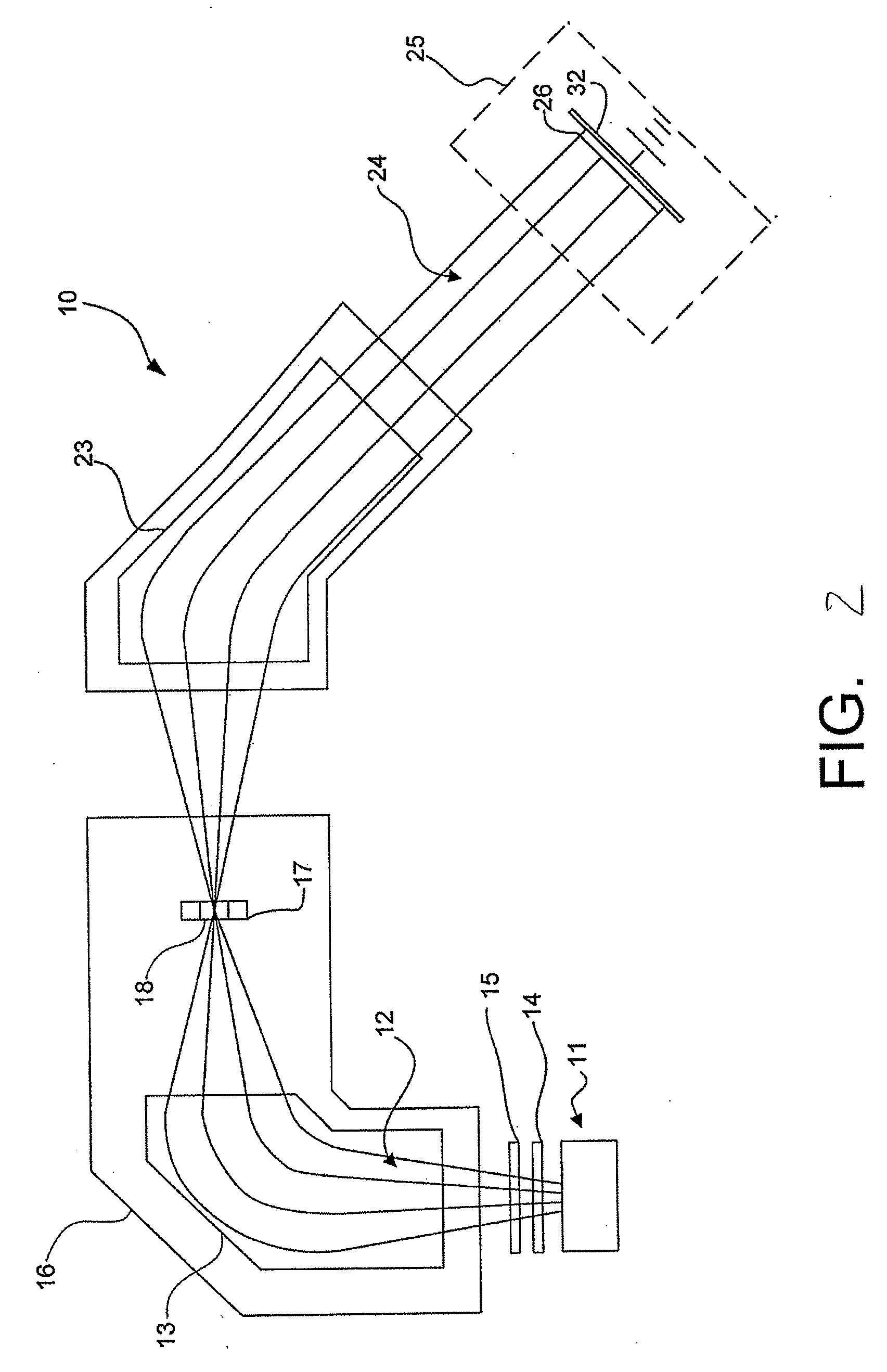
[0019]The present invention will now be described more fully hereinafter with reference to the accompanying drawings, in which preferred embodiments of the invention are shown. This invention, however, may be embodied in many different forms and should not be construed as limited to the embodiments set forth herein. Rather, these embodiments are provided so that this disclosure will be thorough and complete, and will fully convey the scope of the invention to those skilled in the art. In the drawings, like numbers refer to like elements throughout.

[0020]The apparatus and methods are described herein in connection with an ion implanter. However, the methods can be used with other systems and processes involved in semiconductor manufacturing or other systems that use bonding of substrates. Thus, the invention is not limited to the specific embodiments described below. As described above, activation of substrate bonding surfaces improves the quality of SOI wafers or other products wher...


PUM


Abstract

A method for wafer bonding two substrates activated by ion implantation is disclosed. An in situ ion bonding chamber allows ion activation and bonding to occur within an existing process tool utilized in a manufacturing process line. Ion activation of at least one of the substrates is performed at low implant energies to ensure that the wafer material below the thin surface layers remains unaffected by the ion activation.

Description

STATEMENT REGARDING RELATED APPLICATIONS[0001]This application claims the benefit of priority to U.S. Provisional Application No. 60 / 974,250 entitled “Wafer Bonding Activated By Ion Implantation,” filed Sep. 21, 2007.BACKGROUND OF THE INVENTION[0002]1. Field of the Invention[0003]Embodiments of the invention relate to the field of substrate implantation and bonding. More particularly, the present invention relates to an apparatus and method for ion activation of substrates to facilitate bonding.[0004]2. Discussion of Related Art[0005]Ion implantation is a process used to dope ions into a work piece. One type of ion implantation is used to implant impurity ions during the manufacture of semiconductor substrates to obtain desired electrical device characteristics. As is well known in the art, silicon wafers have a crystalline structure wherein the intrinsic conductivity of the silicon is too low to be a useful electrical device. However, by doping a desired impurity into the crystal l...

Claims


Application Information

Patent Timeline
IPC IPC(8): H01L21/46H01J37/08
CPCH01J37/20H01J37/3171H01J2237/201H01J2237/202H01L2924/30105H01L21/6835H01L21/76251H01L2221/68359H01L21/26506H01L21/26593H01L21/2658H01L21/26566
Inventor EROKHIN, YURISULLIVAN, PAULWALTHER, STEVEN R.NUNAN, PETER
Owner VARIAN SEMICON EQUIP ASSOC INC
Why Eureka
Try Eureka