Method for notch filtering a digital signal, and corresponding electronic device

a digital signal and filtering technology, applied in the field of digital signal processing, can solve the problems of high-order modulator, noise pollution of cellular receive bands, and clock frequency limitation, and achieve the effect of reducing quantization nois

Active Publication Date: 2009-03-26
ST ERICSSON SA
View PDF20 Cites 57 Cited by
  • Summary
  • Abstract
  • Description
  • Claims
  • Application Information

AI Technical Summary

Benefits of technology

[0011]According to an embodiment, a radiofrequency digital to analog converter (DAC) array is used to place notches in the DAC transfer function, thus reducing the quantization noise in critical frequency bands.
[0012]According to another embodiment, it is a much simpler sigma-delta modulator, e.g. one with cascaded first order stages, which can be realized at much higher clock frequencies without increasing too much the power consumption that may be used.
[0015]In other words, instead of one RF DAC, several RF DACs are coupled to a chain of (at least one) delay blocks. The delay blocks operate with the clock used by sigma-delta modulation means or circuitry. Further, the digital to analog conversion means or circuitry may be identical, thus potentially easier to build. And, as the coefficients of the filter are positive, the useful signal amplitude is the sum of the DAC signal amplitudes. There is thus less signal power loss due to negative coefficients.
[0016]The positions of the notches of the notch filter, i.e. the frequencies of the notches are related to the delay values of the delay blocks. Thus, a notch filter is provided whereby the quantization noise in the desired frequency bands is reduced.
[0019]Additional flexibility can be added by making the delays programmable. In this case, an advantageous position of the notches can be chosen as a function of, for example, the transmission carrier frequency, and the actual coexistence uses in the mobile phone. This flexibility reduces further the transmission filtering requirements.

Problems solved by technology

However, in a mobile phone, this kind of noise is polluting the cellular receive bands like the DCS, PCS, or W-CDMA bands.
A drawback of this approach is that the coefficients are implemented by multipliers that may perform the multiplication in a fraction of the sampling clock period.
This leads to a limitation of the clock frequency and, in practice, the highest achievable clock frequency is in the range of 1 GHz when using conventional silicon technologies, like 65 nanometers CMOS.
This limitation means that, to achieve an acceptable noise shaping, a quite high order modulator is needed.
For example, a W-CDMA transmitter architecture needs two 9th order 4-bit modulators to suppress the quantization noise in the W-CDMA Rx band, with an estimated power consumption of 150 mW, which may be too high for mobile applications.
However, such an approach also suffers drawbacks.
For example, to achieve a bandpass filter with a relatively narrow band and good attenuation, a great number of FIR elements must be used, with coefficients that vary in a wide range, which may be hard to realize.
As a part of the coefficients may be negative to achieve good bandpass filter characteristics, a part of the radiofrequency power produced by the digital to analog converter may be cancelled, thus the efficiency is not optimal.

Method used


Image

  • Method for notch filtering a digital signal, and corresponding electronic device
  • Method for notch filtering a digital signal, and corresponding electronic device
  • Method for notch filtering a digital signal, and corresponding electronic device

Examples


Embodiment Construction

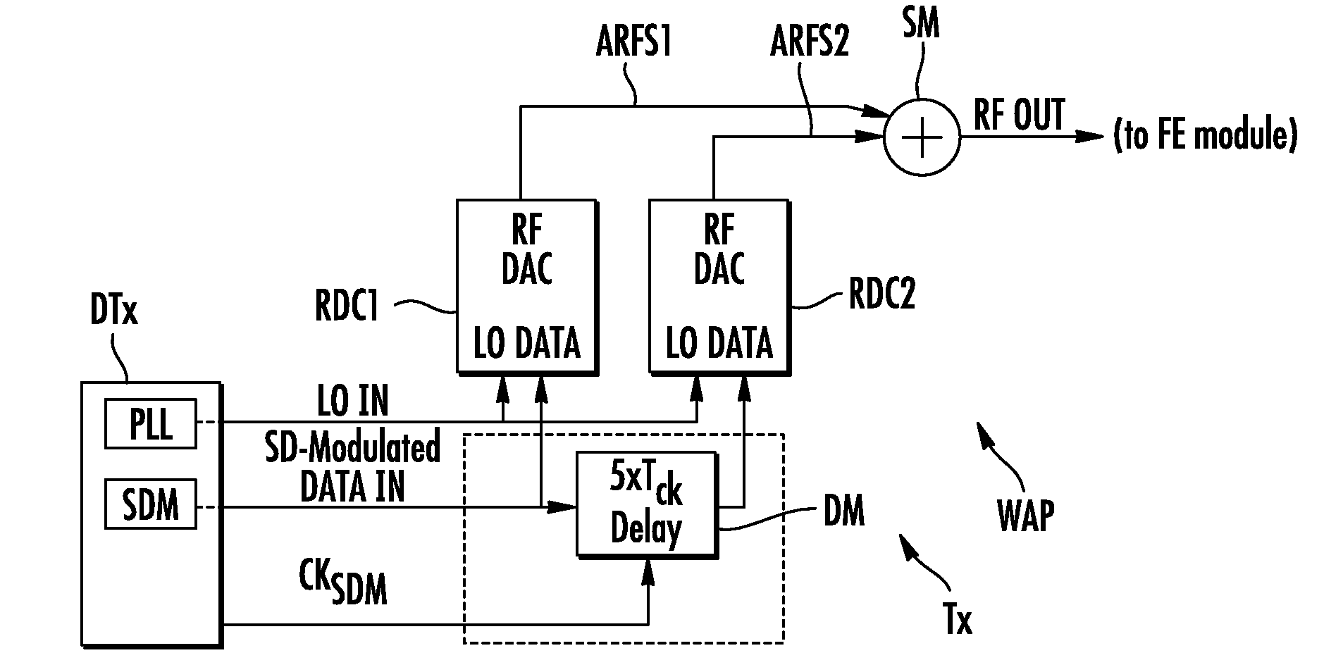
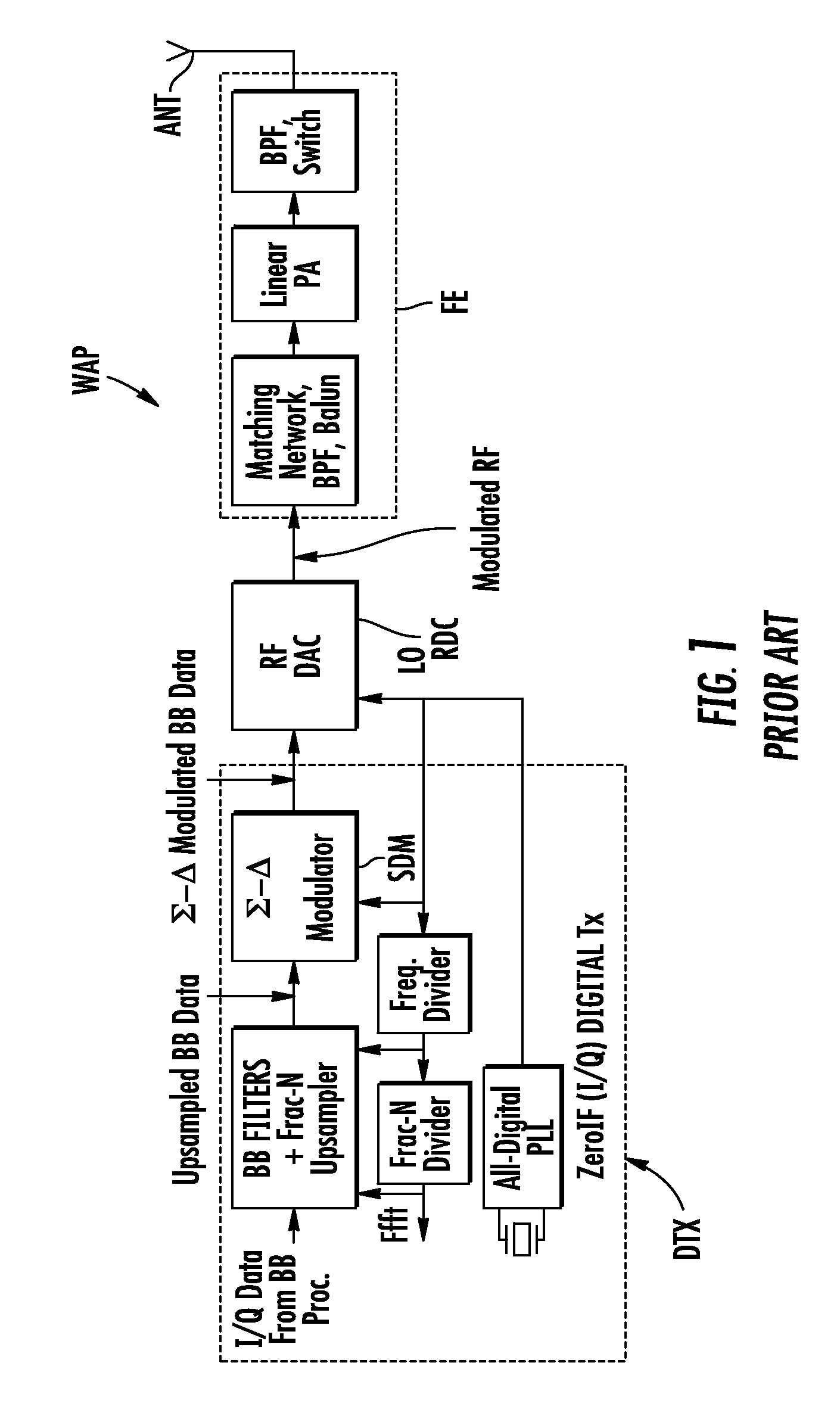
[0029]FIG. 1 illustrates an example of a conventional transmission chain of a wireless apparatus WAP, such as a mobile phone. The transmission chain comprises a digital stage DTX connected through a single radiofrequency digital to analog converter RDC, to an analog front end stage FE. The front end stage FE is connected to an antenna ANT.

[0030]The digital stage DTX comprises low and high frequency digital logic, whose task is to change the sampling rate of the base-band (BB) signal delivered by a base-band processor, from Ffft (Base-Band Sampling Frequency, in the range of a few MHz) to Fc (Fcarrier) or a multiple of Fc, in the range of a few hundred MHz to a few GHz. This upsampled signal is then processed by a sigma-delta modulator (SDM) in order to represent the high resolution base-band signal using a reduced number of bits.

[0031]The front end stage comprises conventionally a matching network, bandpass filter (BPF), balun, as well as a linear power amplifier (PA) and other conv...


PUM


Abstract

An electronic device, includes sigma-delta modulation circuit to operate with a clock signal and having output circuitry to deliver a digital data signal. First circuitry delivers a radiofrequency transposition signal. A notch filter includes radiofrequency digital-to-analog conversion blocks, having first input circuitry coupled to the output circuitry. Second input circuitry receives the radiofrequency transposition signal. Second output circuitry delivers a radiofrequency analog signal. Digital delay circuitry is controlled by the clock signal and includes a delay block between the two first input circuits. The frequency of a notch of the notch filter is related to the value of the delay from the delay block. Summation circuitry sums the radiofrequency signals.

Description

FIELD OF THE INVENTION[0001]The invention relates to the processing of digital signals, in particular the notch filtering of such signals delivered by sigma-delta modulation in order to reduce the quantization noise in certain frequency bands.[0002]A non-limiting application of the invention is directed to a wireless apparatus, in particular cellular mobile phones, operating with two or more radio systems simultaneously, for example one connectivity system like WiFi or WiMAX, and one cellular system in the DCS, PCS or W-CDMA bands.BACKGROUND OF THE INVENTION[0003]Generally speaking, the transmission chain of a wireless apparatus, like a mobile phone, comprises a digital stage and an analog front-end-module coupled to an antenna. The digital stage and the front-end module are mutually coupled through a digital to analog conversion stage.[0004]In order to reduce the number of bits in the digital to analog conversion stage, a high frequency sigma-delta modulator is used.[0005]Due to th...

Claims


Application Information

Patent Timeline
Patent Type & Authority Applications(United States)
IPC IPC(8): H04W99/00
CPCH03H17/025H03M3/504
Inventor POZSGAY, ANDRASPAILLARDET, FREDERIC
Owner ST ERICSSON SA
Why Eureka
Try Eureka